TIDT412A October 2024 – November 2024
3.2 Output Voltage Transitions
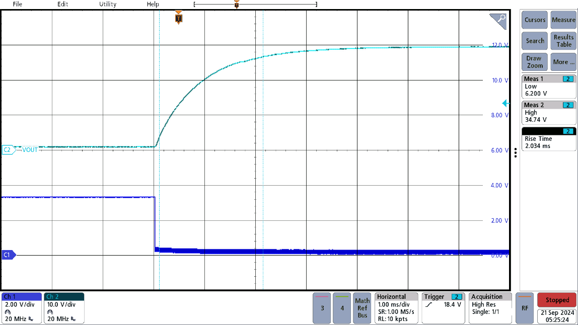
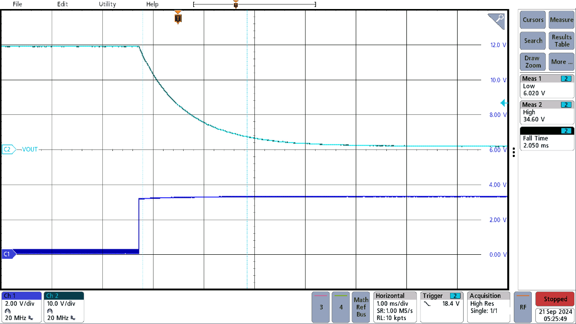
Figure 3-3 and Figure 3-4 show how the output voltage transitions from 6V to 35V and from 35V to 6V respectively with an input voltage of 48V, and with a 2.5Ω load. No significant overshoot was observed.
The PWM signal is included in the measurements on channel 1 to show what is triggering this voltage change. Although the PWM signal looks as though the signal transitions from a constant 3.3V to a constant 0V, this is a product of the 1ms timescale that is used to show the output voltage transition. In reality, the constant 3.3 portion just has a very high duty cycle, while the constant 0 has a very low duty cycle.
 Figure 3-3 6V to 35VOUT Transition With 2.5Ω
Load
 Figure 3-4 35V to 6VOUT Transition with 2.5Ω
Load