TIDT412A October 2024 – November 2024
3.1 Switching
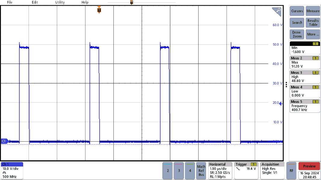
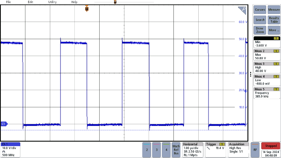
Figure 3-1 and Figure 3-2 show the switching waveforms across different output voltages, but all use an input voltage of 48V, and a resistive load of 2.5Ω. These signals were measured at the source pins of the high-side power stage FETs (Q5 and Q6) but only one waveform is shown, as operation is similar across the FETs. Additionally, a tip and barrel probe was used for this measurement, with the tip at the source pins of the FET and the barrel at the GND of the nearby input capacitors.
Figure 3-1 was taken with an output voltage of 6V and has an overshoot of 3.2V above the 48V input voltage, while Figure 3-2 with an output voltage of 20V has an overshoot of 2.8V above of the 48V input voltage. This is well within the 60V drain-to-source voltage rating of the FET.
 Figure 3-1 6VOUT Switching
Waveform
 Figure 3-2 20VOUT Switching
Waveform