TIDUAH1A August 2015 – April 2018
2.4.3 Digital Output Drivers
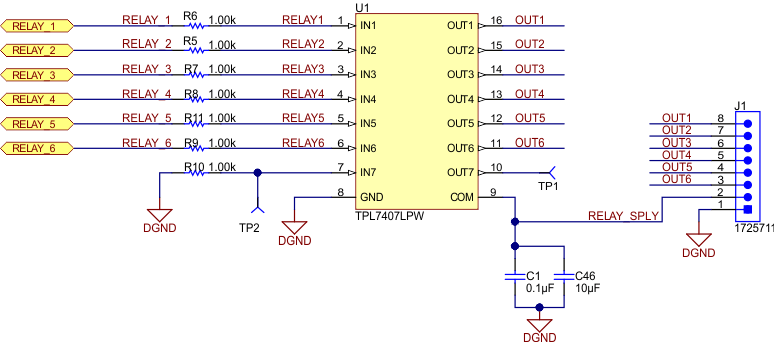
This TI Design provides six high-current digital output drivers. The design features a TPL7407L low-side relay driver. The key benefit of the TPL7407L relay driver is its improved power efficiency and lower leakage in comparison to a bipolar Darlington implementation. The per channel rated drain current capacity of the TPL7407L device is 600 mA.
The COM pin is the power supply pin of TPL7407L to power the gate drive circuitry. This design ensures a full-drive potential with any GPIO above 1.5 V. The gate drive circuitry is based on low-voltage CMOS transistors that can only handle a max gate voltage of 7 V. An integrated LDO reduces the COM voltage of 8.5 V to 40 V to a regulated voltage of 7 V. Though TI recommends an 8.5-V minimum for VCOM, the part still functions with a reduced COM voltage, a reduced gate drive voltage, and a resulting higher Rdson.
To prevent overvoltage on the internal LDO output because of a line transient on the COM pin, the COM pin must be limited to below 3.5 V/μs. TI recommends to use a bypass capacitor that limits the slew rate to below 0.5 V/μs.
The TPL7407L relay driver outputs are controlled by the MSP430F67791A port pins, as the following Figure 14 shows.
 Figure 14. Digital Output Driver Circuit