TIDUCJ0G November 2016 – April 2020
6.4.1.5 Running Code (Build 1)
- Run the project by clicking on
 .
. - In the watch view, periodically check if theguiVbus(VIENNA_guiVbus_Volts in the expression window) variable is updating. If there is no change in the value then make sure the real-time mode is enabled, and the HW is setup correctly. Do not proceed further unless the update is verified.
- Note: As no power is applied right now, this value will be close to zero.
- Now slowly increase the input AC voltage from 0 to 120-Vrms L-N.
- Verifying the voltage sensing: Make sure guiVbus, guiVbusPM, and guiVbusMN display the correct values. For the 120-Vrms L-NguiVbus will be close to 320 V, and the guiVbusPM/MN will be close to 160 V each. The code runs a sine analyzer module, which computes the RMS value of the voltage and current. Notice the value of guiVrms1/2/3 will be close to the input value, that is, 120Vrms. This verifies the voltage sensing of the board.
- Verifying the current sensing: Notice theguiIrms1/2/3, for the given test condition this value will be close to 0.92 Amps. Additionally, the graphs must be seen to verify the current measurement. Below the test condition they will look as shown in Figure 23.
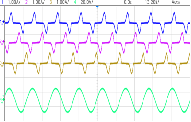
- The scope capture of the input voltage and currents is shown in Figure 24.
- Next to verify the PWM action, first reduce the input voltage to zero and wait for all the voltages to go down to zero.
- Now set the dutyPU_DC to 0.5 in the expressions view.
- Next clear the PWM trip by writing a 1 to clearTrip.
- Slowly increase the input voltage, and keep watch on the input current. The duty cycle will impart a boost action. For example, when Vac is 30 Vrms without switching enabled, the guiVbus will be ~84 V; with switching, the guiVbus will rise up to 140 V. Thus, guiVbusPM/MN will also be higher than the input voltage maximum.
- Below the test conditions described in this build, the guiVbus will rise to about 600 V and guiVbusPM/MN will be close to 300 V each, and the current will be close to 2.8 Vrms when the input voltage reached 120 Vrms L-N. Expressions view will appear as shown in Figure 25. Make sure all the variables are accurate, that is, guiVrms1/2/3, guiIrms1/2/3, guiPF1/2/3. If any variable is not in line with as shown in Figure 25, it points to a hardware issue with the sensing circuit. The scope capture is shown in Figure 26.
- This check verifies at a basic level the PWM driver and connection on hardware.
- Reduce the input voltage to zero, and watch for the bus voltages to reduce down to zero.
- This completes the check for this build, the following items are verified on successful completion of this build:
- Sensing of voltages and currents and scaling to be correct
- Interrupt generation and execution of the build 1 code in the controlISR and tenkHzISR()
- PWM driver and switching
- The controller can now be halted, and the debug connection terminated.
- Fully halting the MCU when in real-time mode is a two-step process. First halt the processor by using the Halt button on the toolbar (
 ) or by using Target > Halt. Then take the MCU out of real-time mode by clicking on
  . Finally, reset the MCU by clicking on
  .
. - Close CCS debug session by clicking on Terminate Debug Session (Target > Terminate all).

Figure 23. Build Level 1: Graph1.GraphProp and Graph2.GraphProp Files Showing Measured Voltage and Currents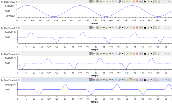

Figure 24. Build Level 1: Scope Capture IL1, IL2, IL3 and V1 (120Vrms L-N) With PWM Tripped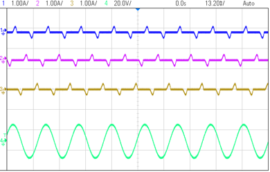

Figure 25. Build Level 1: Expressions View With Power Measurement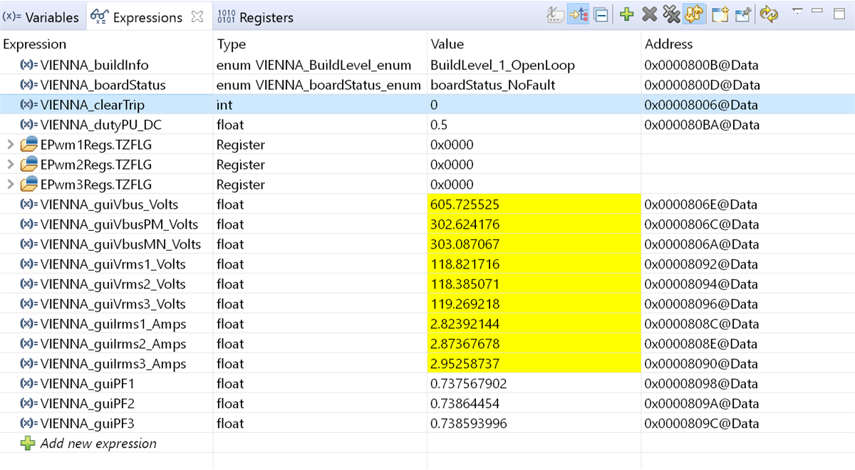

Figure 26. Build Level 1: Scope Capture IL1, IL2, IL3 and V1 (120-Vrms L-N) With Duty Cycle 0.5