TIDUCJ0G November 2016 – April 2020
6.4.2.4 Running Code (Build 2)
- Run the project by clicking
 .
. - It is advisable to test first at a low voltage. Therefore, the input AC voltage is raised to only 40 Vrms, 60 Hz.
- The input current and voltage will look like Figure 30.
- A current reference is set by changing the iLRef variable in the expressions view. This variable is set to 0.05.
- Clear the trip by setting the clearTrip variable to 1.
- As soon as the trip is cleared, a sinusoidal current will be seen to be drawn from the input, which verifies correct operation of the current loop. The waveform will look like Figure 31.
- The guiVbus will be close to 190 V, and the input AC current per phase will be close to 0.6 Amps
- Raise the current reference iLRef to 0.1. Observe the bus voltage to go to 266 V and the input current to around 1.2 Amps.
- Now raise the input AC voltage slowly to 120 Vrms. The board will maintain the input current to be constant as the input voltage rises.
- When the input has stabilized to 120 Vrms, raise the iLRef so the guiVbus is 600 V; for the test conditions specified, this will correspond to iLRef = 0.165. The current waveforms will look like Figure 32.
- As only a proportional gain is used in the compensator, the current reference minus the feedback error is never zero. Notice the current drawn to deviate slightly from the reference.
- SFRA is integrated in the software of this build to verify the designed compensator provides enough gain and phase margin by measuring on hardware. To run the SFRA keep the project running, and from the syscfg page, click on the SFRA icon. SFRA GUI will pop-up.
- Select the options for the device on the SFRA GUI. For example, for F28379D select floating point. Click Setup Connection. On the pop-up window uncheck the boot on connect option, and select an appropriate COM port. Click OK. Return to the SFRA GUI, and click Connect.
- The SFRA GUI will connect to the device. A SFRA sweep can now be started by clicking Start Sweep. The complete SFRA sweep will take a few minutes to finish. Activity can be monitored by seeing the progress bar on the SFRA GUI and also checking the flashing of blue LED on the back on the control card that indicates UART activity. When complete, a graph with the open loop plot will appear, as in Figure 33. This verifies that the designed compensator is indeed stable.
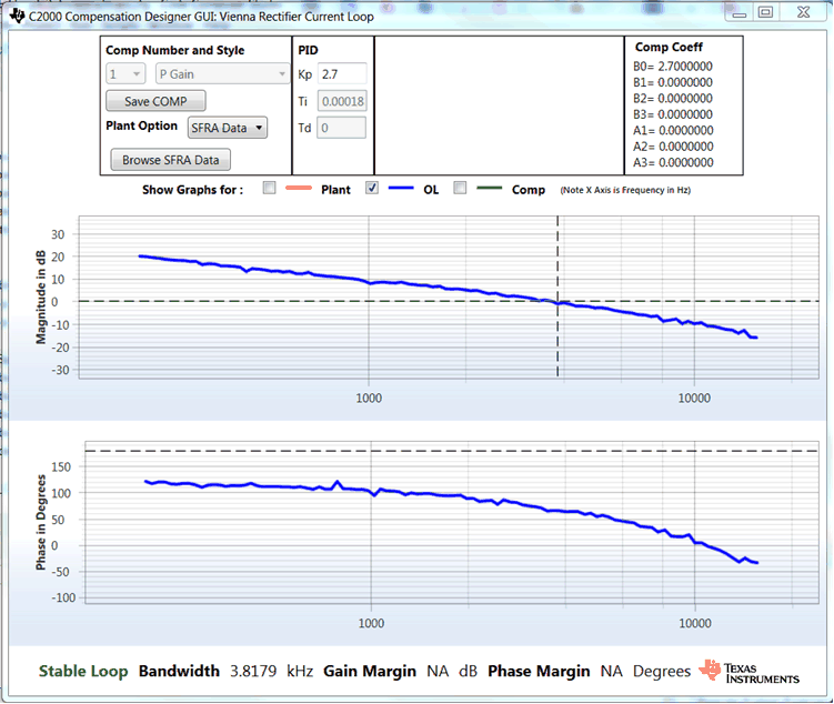
- Click the Compensation Designer again from the SYSCFG page, and choose SFRA Data for plant option on the GUI. This option will use the measured plant information to design the compensator and can be used to fine tune the compensation. By default the Compensation Designer will point to the latest SFRA run and show up as Figure 35. If a previous SFRA run plant information needs to be used, the user can select the SFRAData.csv file by browsing to it by clicking on Browse SFRA Data. Close Compensation Designer to return to the syscfg page when this is done.
- This action verifies the current compensator design. Note the phase if off because there is a negative sign in the control loop.
- To bring the system to a safe stop, bring the input AC voltage down to zero, and observe the guiVBus will come down to zero as well.
- Fully halting the MCU when in real-time mode is a two-step process. First halt the processor by using the Halt button on the toolbar (
 ) or by using Target > Halt. Then take the MCU out of real-time mode by clicking on
  . Finally, reset the MCU (
 ) .
) . - Close the CCS debug session by clicking on Terminate Debug Session (Target > Terminate all).

Figure 30. Build Level 2: Scope Capture IL1, IL2, IL3 and V1 (40Vrms L-N) With PWM Tripped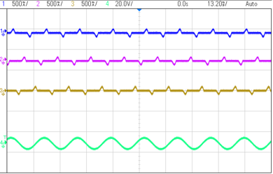

Figure 31. Build Level 2: Scope Capture IL1, IL2, IL3 and V1 (40Vrms L-N) With Current Loop Closed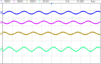

Figure 32. Build Level 2: Scope Capture IL1, IL2, IL3 and V1 (120Vrms L-N) With Current Loop Closed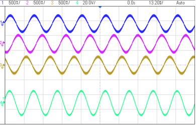

Figure 33. SFRA Run on Closed Current Loop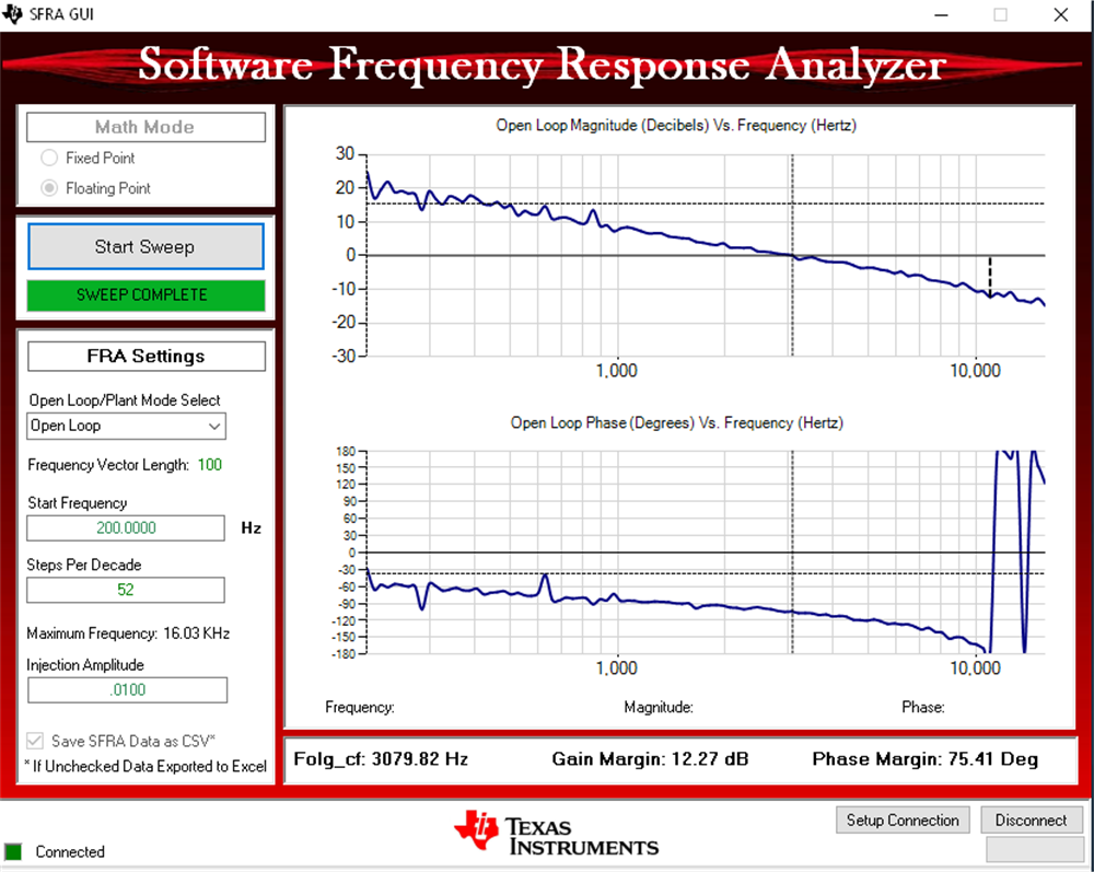

The frequency response data is also saved in the project folder below an SFRA data folder and is time stamped with the time of the SFRA run. Also, note the measured gain and phase margin are close to the modelled values (see Figure 34).
Figure 34. Modelled Versus Measured OL Response for Current Loop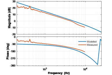

Figure 35. Compensation Designer With Measured Plant Frequency Response Data