TIDUCJ0G November 2016 – April 2020
6.4.3.4 Running Code (Build 3)
- Run the project by clicking
 .
. - Raise the input AC voltage to 120-Vrms VL-N or 208-Vrms VL-L, 60 Hz.
- The DC voltage reference is set by the variable vBusRef. This value is set to as 1.32, which corresponds to 600 V for this design. Refer to calculations.xls sheet for details.
- Clear the trip by setting the clearTrip variable to 1. The bus voltage will then rise to be 600 V.
- Closed loop operation can be verified by comparing the vBusRef and vBusMeas in the expressions window as shown in Figure 39.
- SFRA is integrated in the software of this build to verify the designed compensator provides enough gain and phase margin by measuring on hardware. To run the SFRA, keep the project running, and from the syscfg page, click on the SFRA icon. SFRA GUI will pop up.
- Select the options for the device on the SFRA GUI. For example, for F28379D, select floating point. Click on Setup Connection, and on the pop-up window, uncheck the boot on connect option and select an appropriate COM port. Click OK. Return to the SFRA GUI, and click Connect.
- The SFRA GUI will connect to the device. A SFRA sweep can now be started by clicking Start Sweep. The complete SFRA sweep will take a few minutes to finish. Activity can be monitored by seeing the progress bar on the SFRA GUI and checking the flashing of blue LED on the back on the control card that indicates UART activity. When complete, a graph with the open loop plot will appear, as seen in Figure 40. This action verifies that the designed compensator is indeed stable.
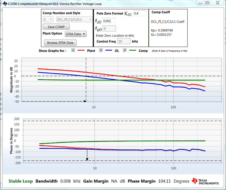
- Click the Compensation Designer again from the SYSCFG page, and choose SFRA Data for plant option on the GUI. This option uses the measured plant information to design the compensator, as shown in Figure 42. This option can be used to fine tune the compensation. By default the Compensation Designer will point to the latest SFRA run. If a previous SFRA run plant information needs to be used, the user can select the SFRAData.csv file by browsing to it by clicking Browse SFRA Data. Close Compensation Designer to return to the syscfg page when done.
- This verifies the voltage compensator design.
- To bring the system to a safe stop bring the input AC voltage down to zero, observe the guiVBus will come down to zero as well.
- Fully halting the MCU when in real-time mode is a two-step process. First halt the processor by using the Halt button on the toolbar (
 ) or by using Target > Halt. Then take the MCU out of real-time mode by clicking on
  . Finally, reset the MCU (
 ).
). - Close CCS debug session by clicking on Terminate Debug Session (Target > Terminate all).

Figure 39. Build Level 3: Expressions Window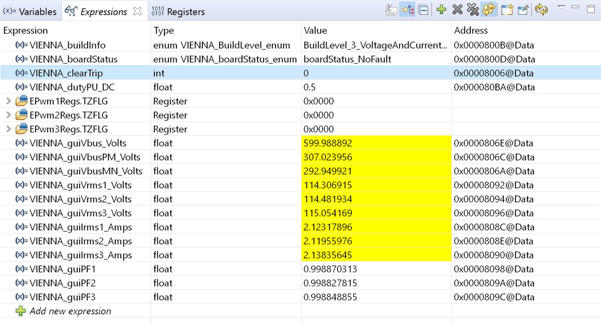

Figure 40. SFRA Run on Closed Voltage Loop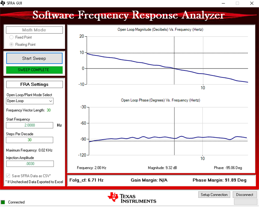

The frequency response data is also saved in the project folder below an SFRA data folder and is time stamped with the time of the SFRA run.
Note the measured gain and phase margin are close to the modelled values, as shown in Figure 41.
Figure 41. Voltage Loop Modeled Versus Measured Comparison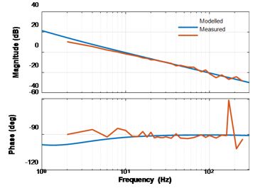

Figure 42. Voltage Loop Compensation Designed With Measured Plant Information