TIDUCL3 February 2017
- 1 Overview
- 2 Resources
- 3 Features
- 4 Applications
- 5 Design Images
- 6 System Overview
-
7 System Design Theory
- 7.1 PCB and Form Factor
- 7.2 Optimizing Board Performance Based on LED String Voltage and Current
- 7.3 Switching Frequency
- 7.4 Output Overvoltage Protection (OVP)
- 7.5 Current Monitoring (IMON)
- 7.6 Thermal Foldback
- 7.7 Clock Generation (PWM)
- 7.8 Onboard Supply and Setting Duty Cycle
- 7.9 Buffering, Averaging, and Filtering
- 7.10 Boost Converter
- 8 Getting Started Hardware
- 9 Testing and Results
- 10Design Files
- 11Related Documentation
- 12About the Author
7.1 PCB and Form Factor
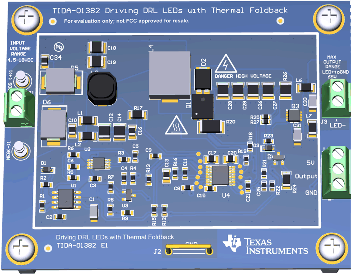
This TI Design is not intended to fit any particular form factor. The specific and primary objective of the design with regards to the PCB is to make a solution that is compact, while still providing a way to test the performance of the board. Figure 7 shows a 3D rendering of the board.
 Figure 7. 3D Render of TIDA-01382 Board
 In a final-production version of this TI Design, several techniques may be used to reduce the size of the solution:
- Test points, headers, sockets, standoffs, and banana plugs can be removed because they do not service a direct function for the board.
- The number, size, and value of capacitors in the system can be optimized.
- The application may not require an input-conducted emissions EMI (PI) filter.