TIDUCL3 February 2017
- 1 Overview
- 2 Resources
- 3 Features
- 4 Applications
- 5 Design Images
- 6 System Overview
-
7 System Design Theory
- 7.1 PCB and Form Factor
- 7.2 Optimizing Board Performance Based on LED String Voltage and Current
- 7.3 Switching Frequency
- 7.4 Output Overvoltage Protection (OVP)
- 7.5 Current Monitoring (IMON)
- 7.6 Thermal Foldback
- 7.7 Clock Generation (PWM)
- 7.8 Onboard Supply and Setting Duty Cycle
- 7.9 Buffering, Averaging, and Filtering
- 7.10 Boost Converter
- 8 Getting Started Hardware
- 9 Testing and Results
- 10Design Files
- 11Related Documentation
- 12About the Author
7.6.2 Thermal Foldback Without PWM Dimming
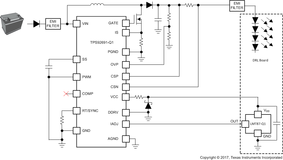
If precision PWM dimming is not required in the application, thermal foldback can still be implemented. The first way to achieve this is adding a bias resistor and a Zener diode to power the LMT87-Q1 from the output of the internal LDO of the TPS92691-Q1. These devices allow the capability of thermal foldback without PWM dimming and without an MCU. Figure 15 is a diagram of this schematic.
 Figure 15. Thermal Foldback Without PWM Dimming
 In this application, the COMP pin is disconnected internally so it does not matter, while the DDRV pin is connected to ground. The VCC pin needs to be connected through a bias resistor to a Zener diode because the output of the internal LDO, VCC, is a constant 7.5 V while the maximum input voltage for the LMT87-Q1 is 5.5 V. Because the current consumption of the LMT87-Q1 is a maximum of 9 µA across temperature, the minimum value of the bias resistor can be calculated. All calculations must be made for a worst case scenario so that the LMT87-Q1 will be powered whenever the output of the internal LDO is regulating. The maximum VCC is 8 V and the minimum voltage needed to power the LMT87-Q1, but still maintain the minimum operating temperature, is 3.5 V. Therefore, the Zener diode is chosen to be somewhere between 3.5 and 5.5 V. Next, take the minimum value of the Zener diode output with respect to its swing across temperature, and subtract it from the max VCC. That value is then divided by the maximum current required to operate the LMT87-Q1 (9 µA) plus the minimum current required to keep the Zener regulating. Equation 15 gives a minimum value of the bias resistor because it ensures the Zener diode to be regulating when the LDO is regulating as shown in Equation 15.

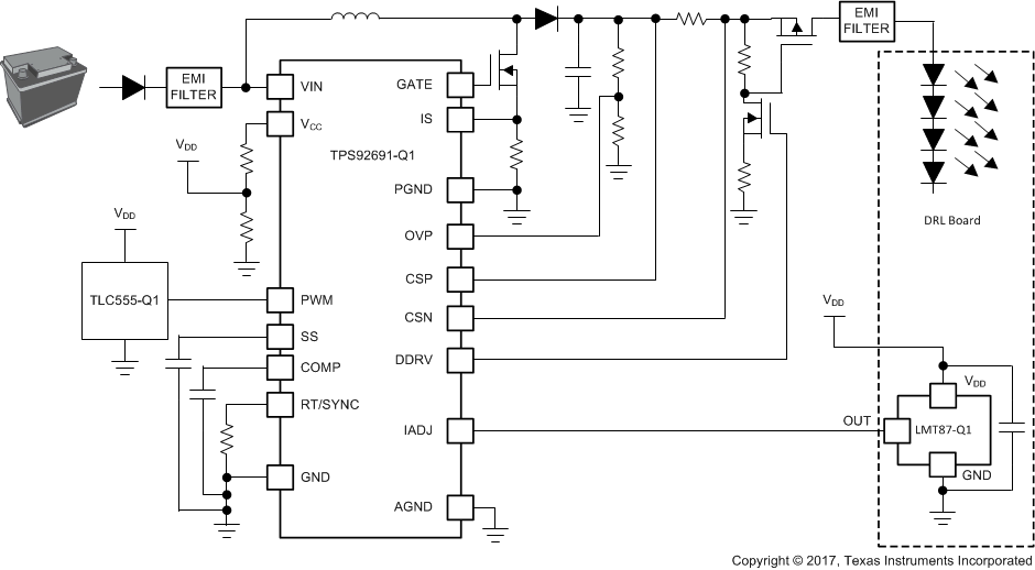
If PWM dimming is required but precision is not, thermal foldback can still be achieved with this TI Design. The schematic reduces to Figure 16.
 Figure 16. Thermal Foldback With PWM Dimming
 The TLC555-Q1 is generating an approximate PWM signal that goes through a low-pass filter into the PWM pin. This signal causes the DDRV pin to PWM dim the output as in the original design. However, in this application, the LMT87-Q1 is being powered by a resistor divided output of the internal LDO. This allows a reduction of parts while still implementing accurate thermal foldback.