TIDUEB2A July 2022 – July 2022
- Description
- Resources
- Features
- Applications
- 5
- 1System Description
-
2System Overview
- 2.1 Block Diagram
- 2.2
Design Considerations
- 2.2.1 Power Multiplexing Circuit Design Parameters
- 2.2.2 Input Connections and Filter
- 2.2.3 Reverse Polarity Protection
- 2.2.4 Battery Charger Input
- 2.2.5 Battery Ideal Diode-OR
- 2.2.6 Input and Battery Switchover Mechanics
- 2.2.7 LM74800 (U1) HGATE
- 2.2.8 Battery LM74800 HGATE
- 2.2.9 BQ25731 Design Considerations
- 2.2.10 BQ25731 Component Selection
- 2.2.11 ILIM Circuit
- 2.2.12 MCU and I2C Bus Design Considerations
- 2.2.13 MSP430FR2475
- 2.2.14 I2C Bus Overview
- 2.2.15 MSP430 Connectors
- 2.2.16 MSP430 Power Supply
- 2.2.17 Sensing Circuits
- 2.2.18 Current Sensing
- 2.2.19 Voltage Sensing
- 2.2.20 Input Comparators
- 2.2.21 Software Flow Chart
- 2.3 Highlighted Products
- 3Hardware, Testing Requirements, and Test Results
- 4Design and Documentation Support
- 5Revision History
2.2.20 Input Comparators
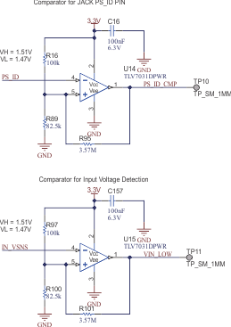
Two comparators are included to monitor VIN_FLT and PS_ID. These signals can be used to provide interrupt generation for the MCU when a specific type of adapter has been inserted or if an input adapter voltage threshold has been met. The TLV7031 nano-power, low-voltage comparator is used to provide a small footprint and low power draw while waiting for input events. Because these devices are powered by the battery when no input adapter is present, the ultra-low quiescent current of 315 nA is a key design feature.
 Figure 2-9 Input Capacitor
Schematic
Figure 2-9 Input Capacitor
SchematicThe voltage setting and hysteresis for
these comparators can be calculated and adjusted according to
Equation 7.