TIDUEB2A July 2022 – July 2022
- Description
- Resources
- Features
- Applications
- 5
- 1System Description
-
2System Overview
- 2.1 Block Diagram
- 2.2
Design Considerations
- 2.2.1 Power Multiplexing Circuit Design Parameters
- 2.2.2 Input Connections and Filter
- 2.2.3 Reverse Polarity Protection
- 2.2.4 Battery Charger Input
- 2.2.5 Battery Ideal Diode-OR
- 2.2.6 Input and Battery Switchover Mechanics
- 2.2.7 LM74800 (U1) HGATE
- 2.2.8 Battery LM74800 HGATE
- 2.2.9 BQ25731 Design Considerations
- 2.2.10 BQ25731 Component Selection
- 2.2.11 ILIM Circuit
- 2.2.12 MCU and I2C Bus Design Considerations
- 2.2.13 MSP430FR2475
- 2.2.14 I2C Bus Overview
- 2.2.15 MSP430 Connectors
- 2.2.16 MSP430 Power Supply
- 2.2.17 Sensing Circuits
- 2.2.18 Current Sensing
- 2.2.19 Voltage Sensing
- 2.2.20 Input Comparators
- 2.2.21 Software Flow Chart
- 2.3 Highlighted Products
- 3Hardware, Testing Requirements, and Test Results
- 4Design and Documentation Support
- 5Revision History
2.2.11 ILIM Circuit
For this design a circuit was added to limit the system current to 8 A. This is most impactful when the device is being used with a 12-V car adapter and can pull the battery voltage below the input threshold of the system. This circuit includes the INA213B to amplify the current across a 2-mΩ sense resistor. This INA213B has a gain of 50 V/V so an input of 8 A results in an 800-mV output.
 Figure 2-4 Current-Limit Circuit
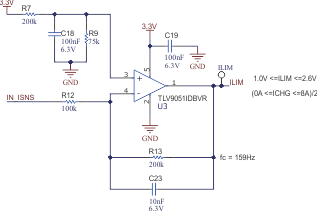
To convert this signal into a usable voltage for the ILIM pin of the BQ25731 devices, an op amp configured as a difference amplifier was used. The voltage on the BQ25731 ILIM pin is converted to charge current based on Equation 5.
where
- IDPM is the target input current limit
- Rac is the 5- or 10-mΩ resistor chosen for the BQ25731
For the difference amplifier when:
where
To correctly set the BQ25731 charge current, set the ILIM pin at 1.0 V with 8 A of system current and 1.8 V with 0-A system current. Limit the charge current for each of the 2 charger devices to between 0 A and 4 A.
Set V2 at 1.8 V in this case. With V2 at 1.8 V, the voltage at the amplifiers positive input is equal to V2/2, which is 0.9 V. This voltage then needs to be created with the system 3.3-V rail and a resistor divider to match the calculated set point. This was implemented with a R7 and R9 as shown in the schematic above.