TIDUEP0 May 2020
- Description
- Resources
- Features
- Applications
- 1Design Images
- 2System Description
-
3System Overview
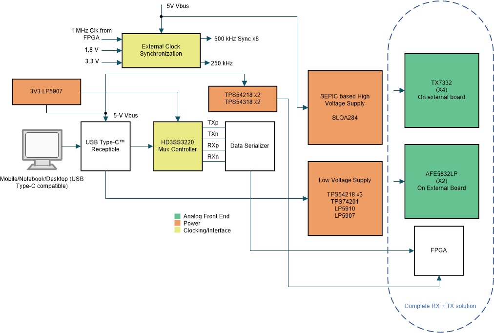
- 3.1 Block Diagram
- 3.2 Design Considerations
- 3.3
Highlighted Products
- 3.3.1 TPD4E05U06 4-Channel Ultra-Low-Capacitance IEC ESD Protection Diode
- 3.3.2 TPD2EUSB30 2-Channel ESD Solution for SuperSpeed USB 3.0 Interface
- 3.3.3 2.3.3 HD3SS3220 10Gbps USB 3.1 USB Type-C 2:1 MUX With DRP Controller
- 3.3.4 TPS54218 2.95V to 6V Input, 2A Synchronous Step-Down SWIFT™ Converter
- 3.3.5 TPS54318 2.95V to 6V Input, 3A Synchronous Step-Down SWIFT™ Converter
- 3.3.6 CSD19538Q3A 100V, N ch NexFET MOSFET™, single SON3x3, 49mOhm
- 3.3.7 LM3488 2.97V to 40V Wide Vin Low-Side N-Channel Controller for Switching Regulators
- 3.3.8 TPS61178 20-V Fully Integrated Sync Boost with Load Disconnect
- 3.3.9 LMZM23601 36-V, 1-A Step-Down DC-DC Power Module in 3.8-mm × 3-mm Package
- 3.3.10 TPS7A39 Dual, 150mA, Wide-Vin, Positive and Negative Low-Dropout (LDO) Voltage Regulator
- 3.3.11 TPS74201 Single-output 1.5-A LDO regulator, adjustable (0.8V to 3.3V), any or no cap, programmable soft start
- 3.3.12 LP5910 300-mA low-noise low-IQ low-dropout (LDO) linear regulator
- 3.3.13 LP5907 250-mA ultra-low-noise low-IQ low-dropout (LDO) linear
- 3.3.14 INA231 28V, 16-bit, i2c output current/voltage/power monitor w/alert in wcsp
- 3.4
System Design Theory
- 3.4.1 Input Section
- 3.4.2
Designing of SEPIC based High Voltage Supply
- 3.4.2.1 Basic Operation Principle of SEPIC Converter
- 3.4.2.2 Design of Dual SEPIC Supply using uncoupled inductors
- 3.4.2.3 Duty Cycle
- 3.4.2.4 Inductor Selection
- 3.4.2.5 Power MOSFET Selection
- 3.4.2.6 Output Diode Selection
- 3.4.2.7 Coupling Capacitor Selection
- 3.4.2.8 Output Capacitor Selection
- 3.4.2.9 Input Capacitor Selection
- 3.4.2.10 Programming the Output Voltage
- 3.4.3 Designing the Low Voltage Power Supply
- 3.4.4 Designing the TPS54218 through Webench Power Designer
- 3.4.5 ± 5V Transmit Supply Generation
- 3.4.6 System Clock Synchronization
- 3.4.7 Power and data output connector
- 3.4.8 System Current and Power Monitoring
- 4Hardware, Software, Testing Requirements, and Test Results
- 5Layout Guidelines
- 6Design Files
- 7Software Files
- 8Related Documentation
- 9About the Author

