TIDUEP0 May 2020
- Description
- Resources
- Features
- Applications
- 1Design Images
- 2System Description
-
3System Overview
- 3.1 Block Diagram
- 3.2 Design Considerations
- 3.3
Highlighted Products
- 3.3.1 TPD4E05U06 4-Channel Ultra-Low-Capacitance IEC ESD Protection Diode
- 3.3.2 TPD2EUSB30 2-Channel ESD Solution for SuperSpeed USB 3.0 Interface
- 3.3.3 2.3.3 HD3SS3220 10Gbps USB 3.1 USB Type-C 2:1 MUX With DRP Controller
- 3.3.4 TPS54218 2.95V to 6V Input, 2A Synchronous Step-Down SWIFT™ Converter
- 3.3.5 TPS54318 2.95V to 6V Input, 3A Synchronous Step-Down SWIFT™ Converter
- 3.3.6 CSD19538Q3A 100V, N ch NexFET MOSFET™, single SON3x3, 49mOhm
- 3.3.7 LM3488 2.97V to 40V Wide Vin Low-Side N-Channel Controller for Switching Regulators
- 3.3.8 TPS61178 20-V Fully Integrated Sync Boost with Load Disconnect
- 3.3.9 LMZM23601 36-V, 1-A Step-Down DC-DC Power Module in 3.8-mm × 3-mm Package
- 3.3.10 TPS7A39 Dual, 150mA, Wide-Vin, Positive and Negative Low-Dropout (LDO) Voltage Regulator
- 3.3.11 TPS74201 Single-output 1.5-A LDO regulator, adjustable (0.8V to 3.3V), any or no cap, programmable soft start
- 3.3.12 LP5910 300-mA low-noise low-IQ low-dropout (LDO) linear regulator
- 3.3.13 LP5907 250-mA ultra-low-noise low-IQ low-dropout (LDO) linear
- 3.3.14 INA231 28V, 16-bit, i2c output current/voltage/power monitor w/alert in wcsp
- 3.4
System Design Theory
- 3.4.1 Input Section
- 3.4.2
Designing of SEPIC based High Voltage Supply
- 3.4.2.1 Basic Operation Principle of SEPIC Converter
- 3.4.2.2 Design of Dual SEPIC Supply using uncoupled inductors
- 3.4.2.3 Duty Cycle
- 3.4.2.4 Inductor Selection
- 3.4.2.5 Power MOSFET Selection
- 3.4.2.6 Output Diode Selection
- 3.4.2.7 Coupling Capacitor Selection
- 3.4.2.8 Output Capacitor Selection
- 3.4.2.9 Input Capacitor Selection
- 3.4.2.10 Programming the Output Voltage
- 3.4.3 Designing the Low Voltage Power Supply
- 3.4.4 Designing the TPS54218 through Webench Power Designer
- 3.4.5 ± 5V Transmit Supply Generation
- 3.4.6 System Clock Synchronization
- 3.4.7 Power and data output connector
- 3.4.8 System Current and Power Monitoring
- 4Hardware, Software, Testing Requirements, and Test Results
- 5Layout Guidelines
- 6Design Files
- 7Software Files
- 8Related Documentation
- 9About the Author
3.4.6 System Clock Synchronization
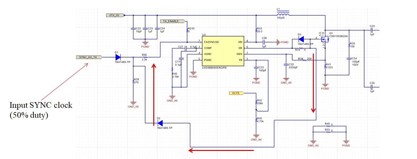
The schematic shown in Figure 11 can be synchronized to an external clock signal only if the duty cycle of the latter is larger than the duty cycle of the controller itself (larger than 93%). This design can be synchronized to an external clock with 50% Duty cycle by implementing the solution shown in Figure 17. The various point of load supplies can be synchronized to external clock which is available on the power connector discussed in section Power and data output connector. The signal from clock source pin DC_DC_CLK_1 is further is divided and distributed to respective supplies supplies and their switching frequencies. Figure 17 shows schematic of the implementation. The source clock is first buffered through LMV112SD and then one output is fed to -5.3V rail at 1 MHz (SYNC -5V_TX) and another one is given as an input to 9Ch-integrated clock buffer and divider device CDCE949. The 8 outputs are 500kHz for the seven TPS54218 buck devices and one TPS61178 for 5V rail, the 9th output is 250kHz for the HV circuit. The configuration of the device CDCE949 can be stored in the integrated EEPROM CDCEL9XXPROGEVM or over I2C. If CDCEL9XXPROGEVM is used, the configuration file can be found in the design files.

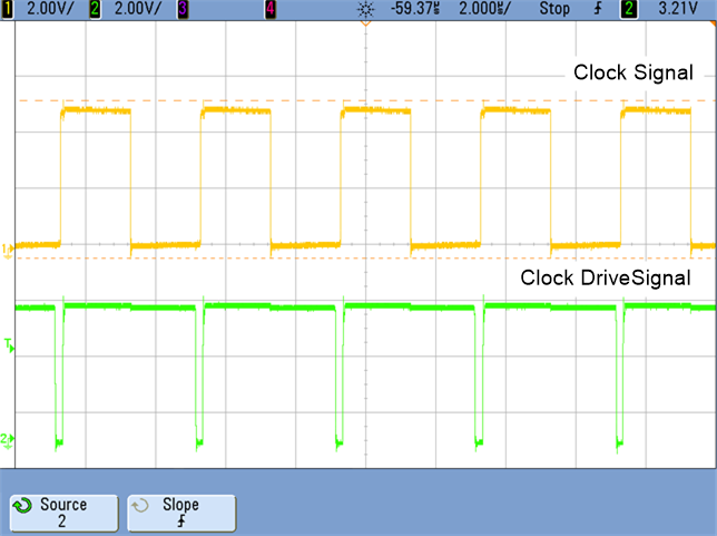
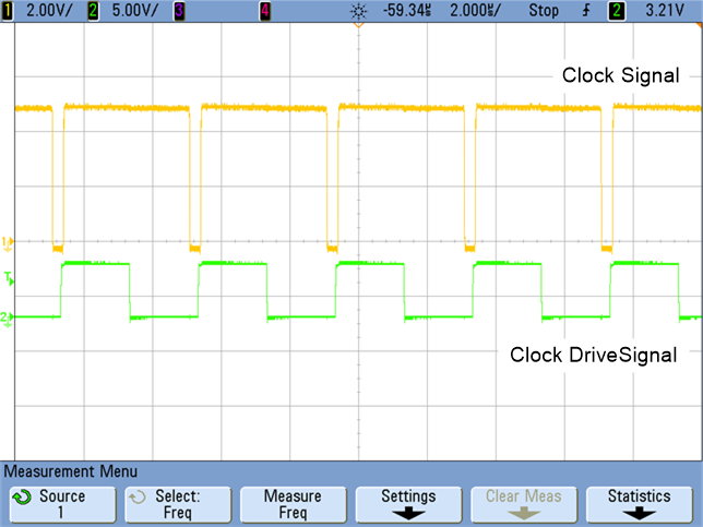
The high voltage circuit can be synchronized to an external clock with 50% duty cycle. The controller LM3488 imposes a limit on the duty cycle clock pulse width to be larger than the duty cycle of the supply which is very high in the current implementation. The schematic shown in Figure 17 depicts the implementation. Two diodes forming an OR-ing system are introduced. One diode is placed from the gate drive pin to the sync pin. The other one comes from the input clock signal. The resistor R36 and R39 are series SYNC resistor and discharge resistor, respectively. If DR_pin is more positive than SYNC_HV_TX, then D1 will be reverse-biased and the SYNC-PIN will be driven high from D2. If DR_pin is less positive than SYNC_HV_TX, then D2 will be reverse-biased and SYNC_PIN will be driven High from D1. Test results are shown in Figure 18 and Figure 19 at the case of no load and full load.

