TIDUEP0 May 2020
- Description
- Resources
- Features
- Applications
- 1Design Images
- 2System Description
-
3System Overview
- 3.1 Block Diagram
- 3.2 Design Considerations
- 3.3
Highlighted Products
- 3.3.1 TPD4E05U06 4-Channel Ultra-Low-Capacitance IEC ESD Protection Diode
- 3.3.2 TPD2EUSB30 2-Channel ESD Solution for SuperSpeed USB 3.0 Interface
- 3.3.3 2.3.3 HD3SS3220 10Gbps USB 3.1 USB Type-C 2:1 MUX With DRP Controller
- 3.3.4 TPS54218 2.95V to 6V Input, 2A Synchronous Step-Down SWIFT™ Converter
- 3.3.5 TPS54318 2.95V to 6V Input, 3A Synchronous Step-Down SWIFT™ Converter
- 3.3.6 CSD19538Q3A 100V, N ch NexFET MOSFET™, single SON3x3, 49mOhm
- 3.3.7 LM3488 2.97V to 40V Wide Vin Low-Side N-Channel Controller for Switching Regulators
- 3.3.8 TPS61178 20-V Fully Integrated Sync Boost with Load Disconnect
- 3.3.9 LMZM23601 36-V, 1-A Step-Down DC-DC Power Module in 3.8-mm × 3-mm Package
- 3.3.10 TPS7A39 Dual, 150mA, Wide-Vin, Positive and Negative Low-Dropout (LDO) Voltage Regulator
- 3.3.11 TPS74201 Single-output 1.5-A LDO regulator, adjustable (0.8V to 3.3V), any or no cap, programmable soft start
- 3.3.12 LP5910 300-mA low-noise low-IQ low-dropout (LDO) linear regulator
- 3.3.13 LP5907 250-mA ultra-low-noise low-IQ low-dropout (LDO) linear
- 3.3.14 INA231 28V, 16-bit, i2c output current/voltage/power monitor w/alert in wcsp
- 3.4
System Design Theory
- 3.4.1 Input Section
- 3.4.2
Designing of SEPIC based High Voltage Supply
- 3.4.2.1 Basic Operation Principle of SEPIC Converter
- 3.4.2.2 Design of Dual SEPIC Supply using uncoupled inductors
- 3.4.2.3 Duty Cycle
- 3.4.2.4 Inductor Selection
- 3.4.2.5 Power MOSFET Selection
- 3.4.2.6 Output Diode Selection
- 3.4.2.7 Coupling Capacitor Selection
- 3.4.2.8 Output Capacitor Selection
- 3.4.2.9 Input Capacitor Selection
- 3.4.2.10 Programming the Output Voltage
- 3.4.3 Designing the Low Voltage Power Supply
- 3.4.4 Designing the TPS54218 through Webench Power Designer
- 3.4.5 ± 5V Transmit Supply Generation
- 3.4.6 System Clock Synchronization
- 3.4.7 Power and data output connector
- 3.4.8 System Current and Power Monitoring
- 4Hardware, Software, Testing Requirements, and Test Results
- 5Layout Guidelines
- 6Design Files
- 7Software Files
- 8Related Documentation
- 9About the Author
5.2 USB Section Layout Guidelines
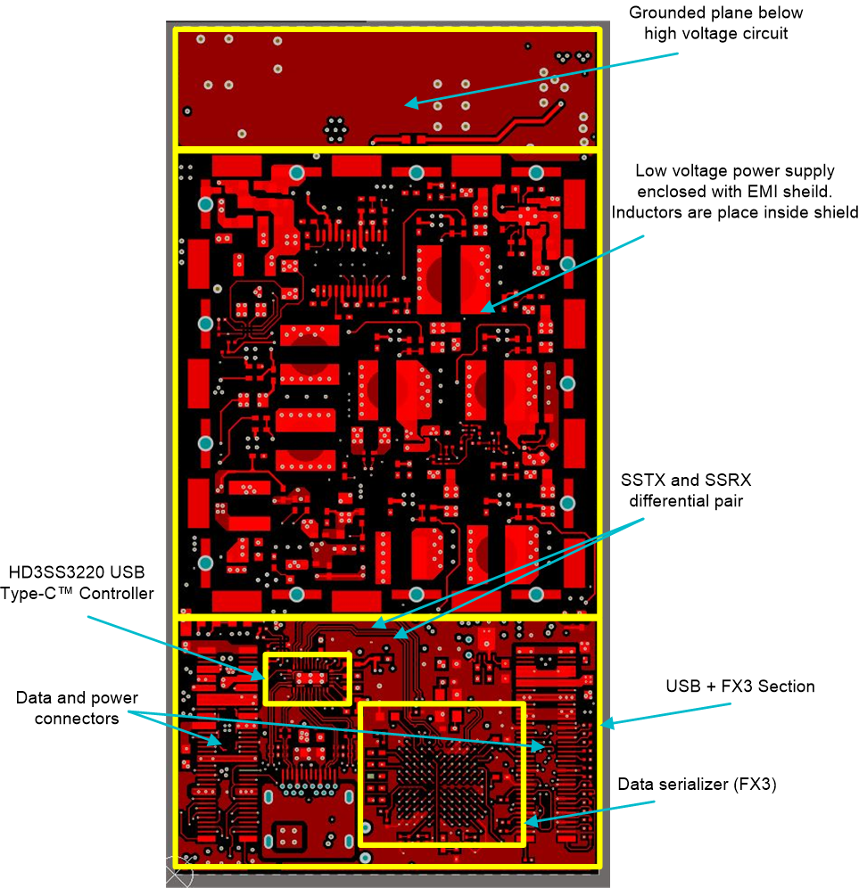
The USB data section comprises of HD3SS3220 Mux controller and FX3 data serializer. Figure 53 shows the routing and placement of the various high speed sections. The device HD3SS3220 has high speed differential signals SSTX and SSRX. The length mismatch should be minimal between these two pair. The design keeps < 3mil length mismatch between these two pair. Figure 53 also shows various other sections of the circuit such as low voltage circuit with the EMI shield placed with all the clocking and LV inductor placed inside. This side faces the TX+RX AFE board hence in order to reduce the EMI noise coupling, a shield is placed between the two. The top most part is a plane comprising the ground of the high voltage circuit. There is no component placed in this region to keep space for the transducer connector and transducer and also to keep a shielding layer from the bottom side.

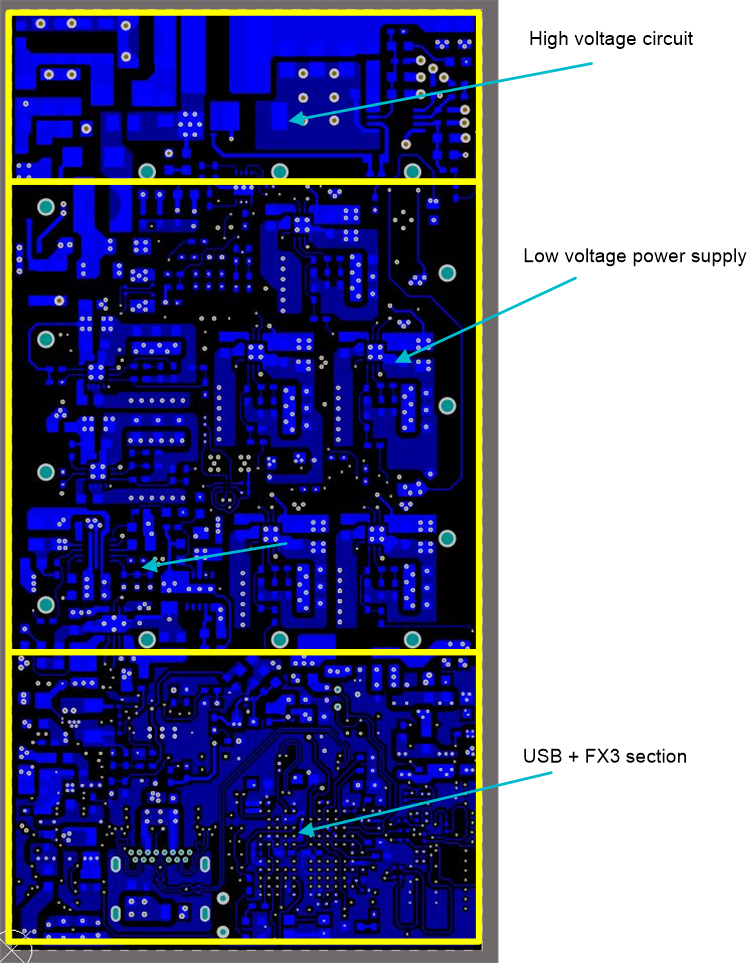
Figure 54 shows the corresponding bottom side of the board highlighting various sections of the board. On this side, at the top, complete high voltage circuit is placed and its layout is discussed separately in Section 5.2.

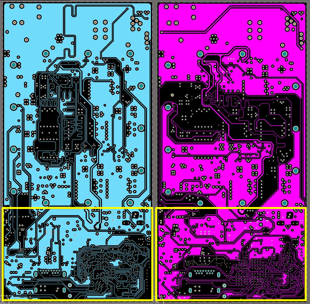
Figure 55 shows the placement and layout of the high-speed 32-bit data signals routed on signal layers. The maximum length of the routed signals is kept 1500 mil with length mismatch of < 100mil. The impedance of the layer is 90 ohm.
