TIDUES6 August 2020 – MONTH
- Description
- Resources
- Features
- Applications
- 5
- 1System Description
- 2System Overview
- 3Hardware, Software, Testing Requirements, and Test Results
- 4Design Files
- 5Software Files
- 6Related Documentation
- 7Terminology
3.1.1 Hardware
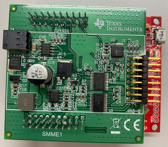
The TIDA-020027 reference design requires the use of the EXP-MSP430F5529LP LaunchPad for full functionality. The design has been outfitted with 2 10 × 2 connectors to connect to the LaunchPad.
The input connector for a typical automotive battery voltage of 12 V and for the LIN bus is provided by jumper J4.
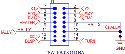
The reference design board provides jumper J2 for the motors, LEDs, heater, and the auto-dimming control signals. Pin 1 is the 3.3-V output of the TLIN1028-Q1 internal LDO output which powers the MSP430 LaunchPad. Pin 15 and 16 are for the hall sensor outputs from the side mirror unit. These hall sensor outputs can be used to implement precise motor positioning and stall detection algorithms.
Jumper J3 contains additional control signals and the SPI communication. Jumper J1 is the output connector where the side mirror unit is connected.
A simple software was developed for the MSP430 MCU to test and validate the board. The firmware monitors and controls the GPIOs which control the different components of the board. The firmware also configures the DRV8873-Q1 and DRV8906-Q1 motor drivers via SPI and monitors the current sense and diagnostic failures.
Figure 3-1, Figure 3-2, and Figure 3-3 show the schematic of the jumper connectors on the board and Figure 3-4 shows an image of the reference design connected to the MSP430 LaunchPad.
 Figure 3-1 J4 Connector
 Figure 3-3 J2 and J3
Connector
 Figure 3-2 J1 Connector
 Figure 3-4 Image of TIDA-020027 Connected to MSP-EXP430F5529LP LaunchPad™