TIDUF99 November 2024
- 1
- Description
- Resources
- Features
- Applications
- 6
- 1System Description
- 2System Overview
- 3System Design Theory
- 4Hardware, Software, Testing Requirements, and Test Results
- 5Design and Documentation Support
- 6About the Author
4.4.3 Bypass Circuit Test Results
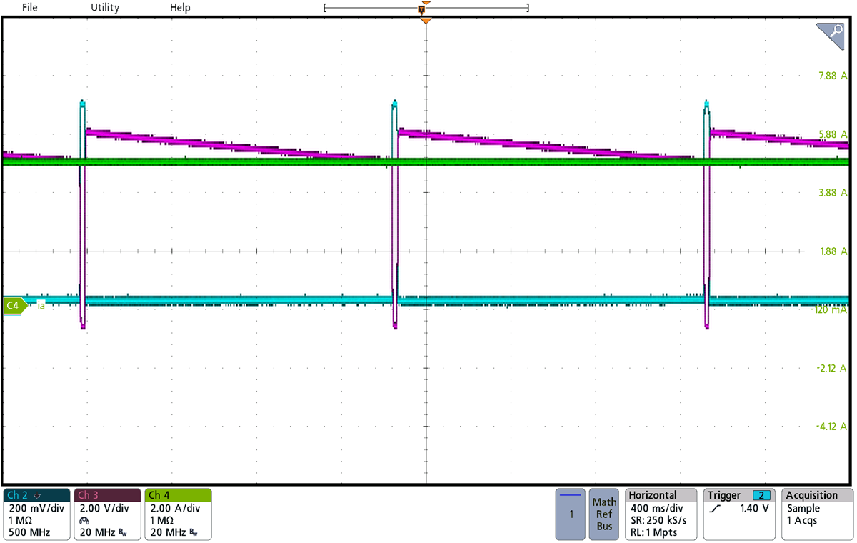
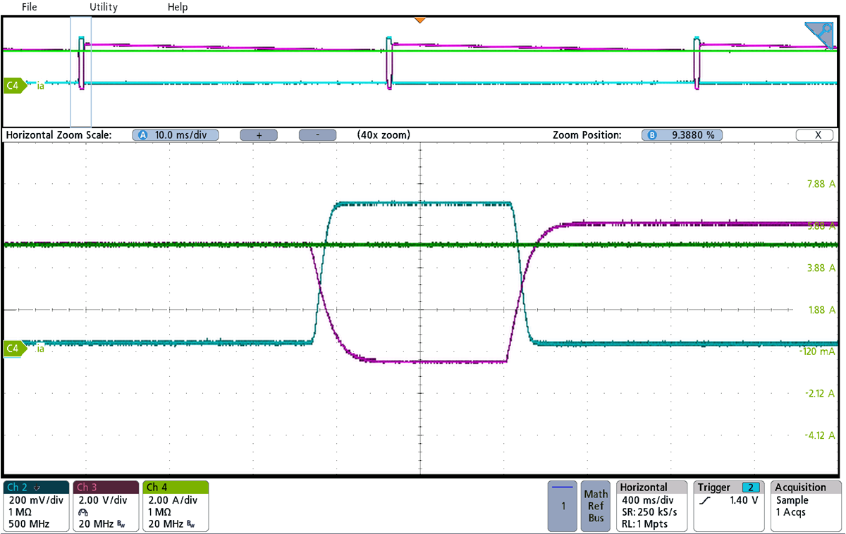
Figure 4-10 and Figure 4-11 show the test result of the bypass circuit based on LM746x0-Q1. Channel 2 is the voltage drop of the bypass circuit. Channel 3 is the gate drive voltage of LM74610-Q1. Channel 4 is the bypass current.
The waveform illustrates that this design can effectively bypass the string current with very low voltage drop and provides around a 98.5% duty cycle. This design reduces the power dissipation and improves the system reliability.
 Figure 4-10 Bypass Circuit Test
Results–Graph A
 Figure 4-11 Bypass Circuit Test
Results–Graph B