TIDUF99 November 2024
- 1
- Description
- Resources
- Features
- Applications
- 6
- 1System Description
- 2System Overview
- 3System Design Theory
- 4Hardware, Software, Testing Requirements, and Test Results
- 5Design and Documentation Support
- 6About the Author
2.2 Design Considerations
The TIDA-010949 board consists of a control card (TMS320F2800137) that gathers data from the panel side, string side, and uses this information to do MPPT and close loop control. The MCU then generates PWM signals that directly drive the half-bridge GaN power stage (LMG2100R026). The buck-boost converter modulates the output voltage of the panel to maximize the transmission power.
To power the system, a 100V switching regulator (LM5164) is used to step down the panel voltage to 12V for PLC. The second fly-buck topology (LMR51410) is used to step down from 12V to a non-isolated 5V and two isolated 5V to provide power for the LMG2100 and C2000 control card. Two isolated 5V is to provide driver voltage for the upper FET of LMG2100 to support 100% duty cycle. From the non-isolated 5V, a low-dropout (LDO) regulator (TPS7A2033) is used to regulate a 3.3V line for the rest of the components.
 Figure 2-2 DC-DC Converter-Buck Stage
 Figure 2-3 DC-DC Converter-Boost Stage
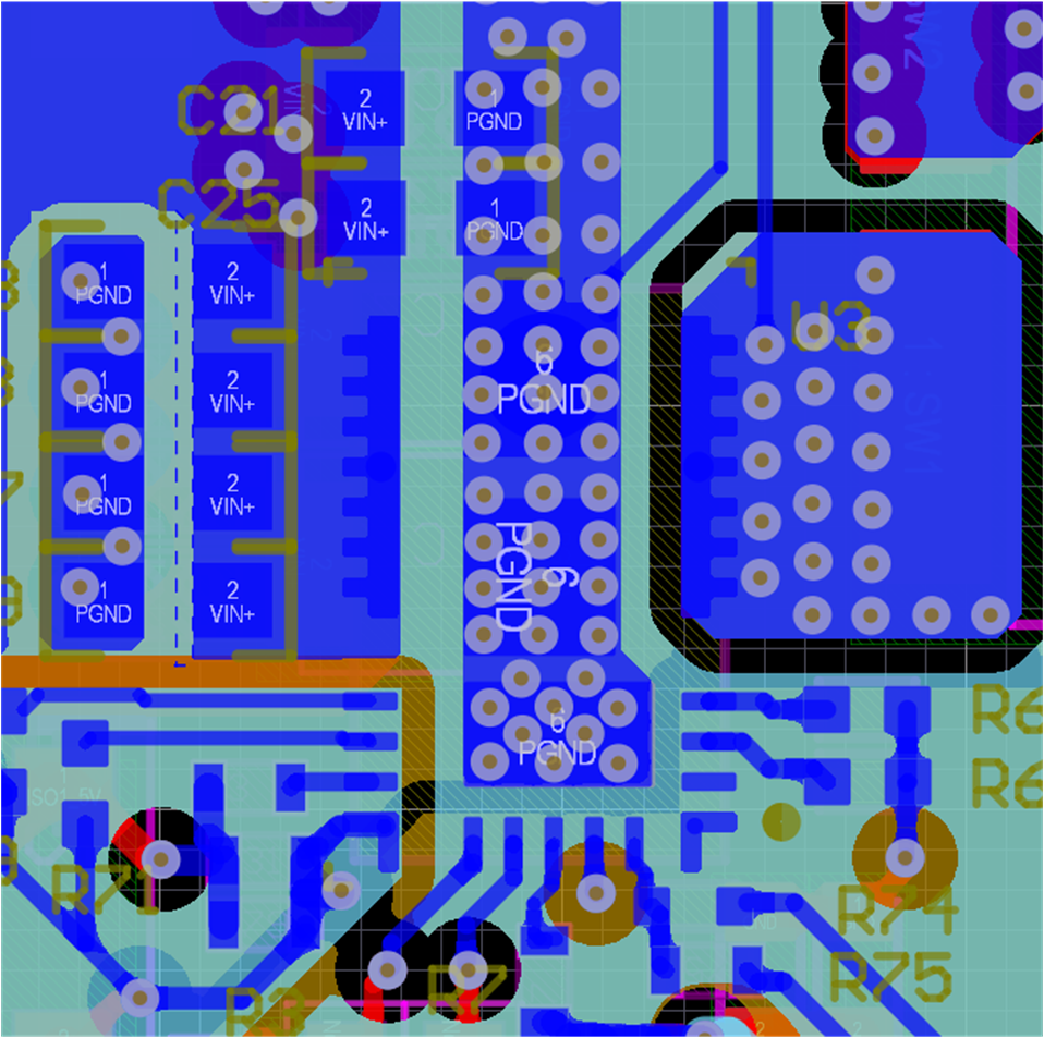
The R6 in the boost stage is a bypass resistor, if the resistor is soldered, then the converter is configured into buck mode. Removing this resistor can configure the converter into 4-switch buck-boost mode. Two LMG2100R026 devices are used in the 4-switch buck-boost power stage. To better utilize the potential of the GaN device, component selection and the layout are important. High-quality input and output MLCCs are needed to better handle the high frequency current during switching. The layout is required to minimized the parasitics in the power loop, thus to reduce the voltage spike and ringing. Short, straight traces produce the lowest impedance path for the signal and minimize the current loop area, thereby reducing loop inductances present. Bypass capacitors filter and condition signals before use and are placed as close to the respective component as possible. Any extraneous trace between the capacitor and component mitigates the effectiveness of the bypass capacitor.
 Figure 2-4 LMG2100R026 Layout
The AFE031 is used for the power line communication interface. This interface includes a power amplifier, PGAs, and filters for the TX and RX path as well as an internal DAC. The SPI to the MCU is used to configure the filters, PGAs, and the internal DAC. For transmitting data, the PWM mode is used. See also the AFE031 Powerline Communications Analog Front-End data sheet for a detailed design description for PWM mode. In the RX path, a band-pass filter is implemented using R58, C87, L5, R59, L6, and C91. This filter removes any noise outside the frequency band used for the PLC communication. The output of the band-pass filter is connected to the internal PGAs and RX filters of the AFE031 and is then connected to an ADC of the MCU, which is sampling and decoding the filtered signal.
The coupling circuit connects the AFE031 to the power line and removes the high voltage to protect the low-voltage circuits of the AFE031. The transformer and DC blocking capacitor in series are in parallel with an LRC circuit. The resonance frequency of this LRC circuit needs to be set to the PLC carrier frequency. This makes sure that there is always sufficient impedance to couple the PLC signal onto the power line and the signal is not shorted through the output capacitor of the power optimizer. R23 sets the impedance at the resonance frequency. L4 needs to handle the full DC current without saturation.
 Figure 2-5 PLC Coupling Circuit
The reference design utilizes J4 and J5 connectors for interfacing the MCU with wireless connectivity modules. These modules add a lot of connectivity options like Wi-SUN®, Zigbee®, Bluetooth® Low Energy, and Wi-Fi®.
The C2000 MCU continuously measures parameters like voltages and currents on input and output and periodically sends this data over universal asynchronous receiver-transmitter (UART). This data can be transmitted over a wireless network to a monitoring system. Also the connectors have dedicated pins to enable rapid shutdown over a wireless network feature.
The wireless connectivity example is available for evaluation by request.
 Figure 2-6 Wireless Connectors