ZHCS036C February 2011 – April 2015 BQ24171
PRODUCTION DATA.
- 1 特性
- 2 应用
- 3 说明
- 4 修订历史记录
- 5 说明(续)
- 6 Device Comparison Table
- 7 Pin Configuration and Functions
- 8 Specifications
-
9 Detailed Description
- 9.1 Overview
- 9.2 Functional Block Diagram
- 9.3
Feature Description
- 9.3.1 Battery Voltage Regulation
- 9.3.2 Battery Current Regulation
- 9.3.3 Battery Precharge Current Regulation
- 9.3.4 Input Current Regulation
- 9.3.5 Charge Termination, Recharge, and Safety Timers
- 9.3.6 Power Up
- 9.3.7 Input Undervoltage Lockout (UVLO)
- 9.3.8 Input Overvoltage/Undervoltage Protection
- 9.3.9 Enable and Disable Charging
- 9.3.10 System Power Selector
- 9.3.11 Converter Operation
- 9.3.12 Automatic Internal Soft-Start Charger Current
- 9.3.13 Charge Overcurrent Protection
- 9.3.14 Charge Undercurrent Protection
- 9.3.15 Battery Detection
- 9.3.16 Battery Short Protection
- 9.3.17 Battery Overvoltage Protection
- 9.3.18 Temperature Qualification and JEITA Guideline
- 9.3.19 MOSFET Short Circuit and Inductor Short Circuit Protection
- 9.3.20 Thermal Regulation and Shutdown Protection
- 9.3.21 Timer Fault Recovery
- 9.3.22 Inductor, Capacitor, and Sense Resistor Selection Guidelines
- 9.3.23 Charge Status Outputs
- 9.4 Device Functional Modes
- 10Application and Implementation
- 11Power Supply Recommendations
- 12Layout
- 13器件和文档支持
- 14机械、封装和可订购信息
10 Application and Implementation
NOTE
Information in the following applications sections is not part of the TI component specification, and TI does not warrant its accuracy or completeness. TI’s customers are responsible for determining suitability of components for their purposes. Customers should validate and test their design implementation to confirm system functionality.
10.1 Application Information
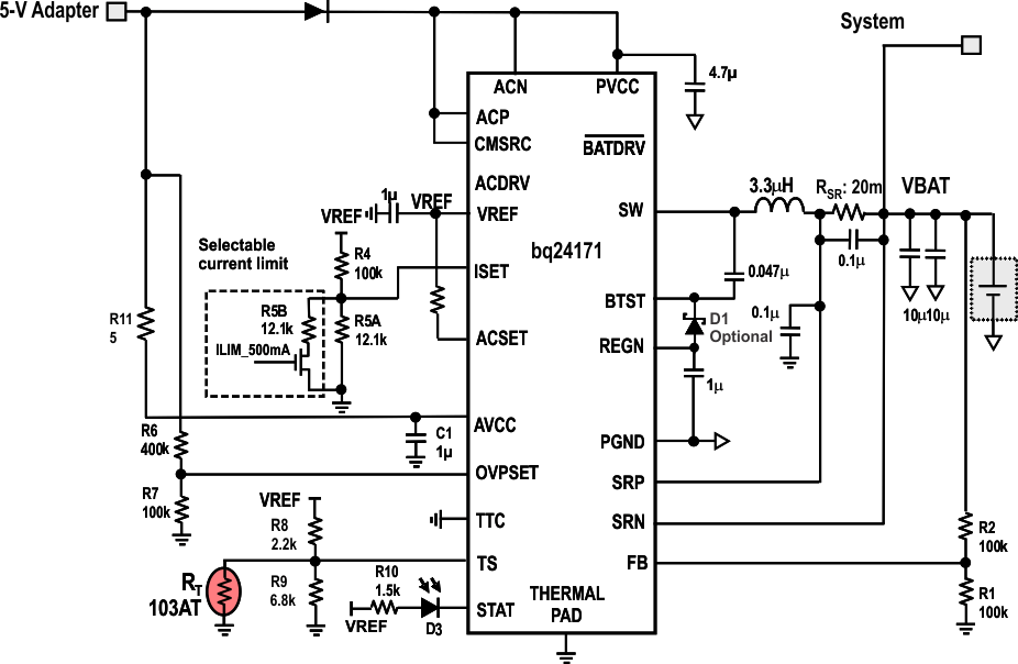
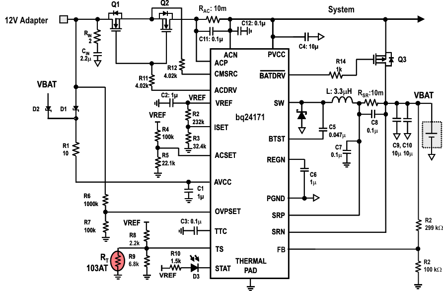
A typical application consists of a bq24171 with power path management and from 1- to 3-cell series Li-ion or Li-polymer battery in a wide variety of portable applications where JEITA-compatible charging limits are desired.
10.2 Typical Application
10.2.1 Design Requirements
For this design example, use the parameters listed in Table 4 as the input parameters.
Table 4. Design Parameters
| PARAMETER | EXAMPLE VALUE |
|---|---|
| Input Voltage Range | 4.5 V - 17 V |
| Input Current DPM Limit | 600 mA min |
| Battery Voltage | 13.5 V max |
| Charge Current | 4 A max |
10.2.2 Detailed Design Procedure
10.2.2.1 Inductor Selection
The bq24171 has a 1600-kHz switching frequency to allow the use of small inductor and capacitor values. Inductor saturation current should be higher than the charging current (ICHG) plus half the ripple current (IRIPPLE):

Inductor ripple current depends on input voltage (VIN), duty cycle (D = VOUT/VIN), switching frequency (fs), and inductance (L):

The maximum inductor ripple current happens with D = 0.5 or close to 0.5. Usually inductor ripple is designed in the range of 20% to 40% of the maximum charging current as a trade-off between inductor size and efficiency for a practical design.
10.2.2.2 Input Capacitor
The input capacitor should have enough ripple current rating to absorb input switching ripple current. The worst case RMS ripple current is half of the charging current when duty cycle is 0.5. If the converter does not operate at 50% duty cycle, then the worst case capacitor RMS current ICIN occurs where the duty cycle is closest to 50% and can be estimated by the following equation:

A low ESR ceramic capacitor such as X7R or X5R is preferred for the input decoupling capacitor and should be placed as close as possible to the drain of the high-side MOSFET and source of the low-side MOSFET. The voltage rating of the capacitor must be higher than the normal input voltage level. A 25-V rating or higher capacitor is preferred for a 15-V input voltage. A 20-μF capacitance is suggested for a typical 3-A to 4-A charging current.
10.2.2.3 Output Capacitor
The output capacitor also should have enough ripple current rating to absorb output switching ripple current. The output capacitor RMS current ICOUT is given as:

The output capacitor voltage ripple can be calculated as follows:

At certain input/output voltages and switching frequencies, the voltage ripple can be reduced by increasing the output filter LC.
The bq24171 has an internal loop compensator. To achieve good loop stability, the resonant frequency of the output inductor and output capacitor should be designed from 15 kHz to 25 kHz. The preferred ceramic capacitor has a 25-V or higher rating, X7R or X5R.
10.2.2.4 Input Filter Design
During adapter hot plug-in, the parasitic inductance and the input capacitor from the adapter cable form a second-order system. The voltage spike at the AVCC pin may be beyond the IC maximum voltage rating and damage the IC. The input filter must be carefully designed and tested to prevent an overvoltage event on the AVCC pin.
There are several methods to damping or limiting the overvoltage spike during adapter hot plug-in. An electrolytic capacitor with high ESR as an input capacitor can damp the overvoltage spike well below the IC maximum pin voltage rating. A high current capability TVS Zener diode can also limit the overvoltage level to an IC safe level. However, these two solutions may not be lowest cost or smallest size.
A cost-effective and small-size solution is shown in Figure 20. R1 and C1 are composed of a damping RC network to damp the hot plug-in oscillation. As a result, the overvoltage spike is limited to a safe level. D1 is used for reverse voltage protection for the AVCC pin. C2 is the AVCC pin decoupling capacitor and it should be placed as close as possible to the AVCC pin. R2 and C2 form a damping RC network to further protect the IC from high dv/dt and high voltage spikes. The C2 value should be less than the C1 value so R1 can dominant the equivalent ESR value to provide enough damping effect for hot plug-in. R1 and R2 must be sized to handle in-rush current power loss according to the resistor manufacturer’s data sheet. Verify the filter component values with a real application and make any minor adjustments needed to fit in the real application circuit.
If the input is 5 V (USB host or USB adapter), diode D1 can be omitted. R2 must be 5 Ω or higher to limit the current if the input is reversely inserted.
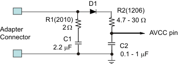 Figure 20. Input Filter
10.2.2.5 Input ACFET and RBFET Selection
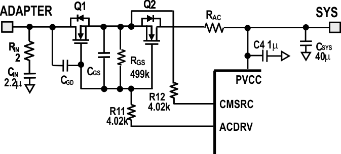
N-type MOSFETs are used as input ACFET(Q1) and RBFET(Q2) for better cost-effective and small-size solution, as shown in Figure 23. Normally, there is a total capacitance of 50 µF connected at PVCC node; 10-µF capacitor for buck converter of bq24171 and 40-µF capacitor for system side. There is a surge current during Q1 turnon period when a valid adapter is inserted. Decreasing the turnon speed of Q1 can limit this surge current in desirable range by selecting a MOSFET with relative bigger CGD and/or CGS. If Q1 turns on too fast, we must add external CGD and/or CGS. For example, 4.7-nF CGD and 47-nF CGS are adopted on EVM while using NexFET CSD17313 as Q1.
10.2.3 Application Curves
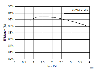 Figure 22. Charge Efficiency
