ZHCS114E march   2011  – february 2023 ADS4222 , ADS4225 , ADS4226 , ADS4242 , ADS4245 , ADS4246

PRODUCTION DATA  

  1. 特性
  2. 应用
  3. 说明
  4. Revision History
  5. 说明(续)
  6. Pin Configuration and Functions
    1.     Pin Functions – LVDS Mode
    2.     Pin Functions – CMOS Mode
  7. Specifications
    1. 7.1  Absolute Maximum Ratings
    2. 7.2  ESD Ratings
    3. 7.3  Recommended Operating Conditions
    4. 7.4  Thermal Information
    5. 7.5  Electrical Characteristics: ADS4246, ADS4245, ADS4242
    6. 7.6  Electrical Characteristics: ADS4226, ADS4225, ADS4222
    7. 7.7  Electrical Characteristics: General
    8. 7.8  Digital Characteristics
    9. 7.9  Timing Requirements: LVDS and CMOS Modes #GUID-C6C0701B-A11B-492F-BD6B-B774F5FE4665/SLAS6895399
    10. 7.10 Serial Interface Timing Characteristics #GUID-3852E7CE-C5B6-42F5-A56A-70AB1B981302/SBAS5097810
    11. 7.11 Reset Timing (Only When Serial Interface Is Used)
    12. 7.12 Typical Characteristics
      1. 7.12.1 ADS4246
      2. 7.12.2 ADS4245
      3. 7.12.3 ADS4242
      4. 7.12.4 ADS4226
      5. 7.12.5 ADS4225
      6. 7.12.6 ADS4222
      7. 7.12.7 General
      8. 7.12.8 Contour
  8. Detailed Description
    1. 8.1 Overview
    2. 8.2 Functional Block Diagrams
    3. 8.3 Feature Description
      1. 8.3.1 Analog Input
        1. 8.3.1.1 Drive Circuit Requirements
        2. 8.3.1.2 Driving Circuit
      2. 8.3.2 Clock Input
      3. 8.3.3 Digital Functions
      4. 8.3.4 Gain for SFDR/SNR Trade-off
      5. 8.3.5 Offset Correction
    4. 8.4 Device Functional Modes
      1. 8.4.1 Power-Down
        1. 8.4.1.1 Global Power-Down
        2. 8.4.1.2 Channel Standby
        3. 8.4.1.3 Input Clock Stop
    5. 8.5 Programming
      1. 8.5.1 47
      2. 8.5.2 Parallel Configuration Only
      3. 8.5.3 Serial Interface Configuration Only
      4. 8.5.4 Using Both Serial Interface and Parallel Controls
      5. 8.5.5 Parallel Configuration Details
      6. 8.5.6 Serial Interface Details
        1. 8.5.6.1 Register Initialization
        2. 8.5.6.2 Serial Register Readout
      7. 8.5.7 Digital Output Information
        1. 8.5.7.1 Output Interface
        2. 8.5.7.2 DDR LVDS Outputs
        3. 8.5.7.3 LVDS Buffer
        4. 8.5.7.4 Parallel CMOS Interface
        5. 8.5.7.5 CMOS Interface Power Dissipation
        6. 8.5.7.6 Multiplexed Mode of Operation
        7. 8.5.7.7 Output Data Format
    6. 8.6 Register Maps
      1. 8.6.1 64
      2. 8.6.2 Description Of Serial Registers
  9. Application and Implementation
    1. 9.1 Application Information
    2. 9.2 Typical Application
      1. 9.2.1 Design Requirements
      2. 9.2.2 Detailed Design Procedure
        1. 9.2.2.1 Analog Input
        2. 9.2.2.2 Clock Driver
        3. 9.2.2.3 Digital Interface
        4. 9.2.2.4 SNR and Clock Jitter
      3. 9.2.3 Application Curves
    3. 9.3 Power Supply Recommendations
      1. 9.3.1 Sharing DRVDD and AVDD Supplies
      2. 9.3.2 Using DC/DC Power Supplies
      3. 9.3.3 Power Supply Bypassing
    4. 9.4 Layout
      1. 9.4.1 Layout Guidelines
        1. 9.4.1.1 Grounding
        2. 9.4.1.2 Supply Decoupling
        3. 9.4.1.3 Exposed Pad
        4. 9.4.1.4 Routing Analog Inputs
      2. 9.4.2 Layout Example
  10. 10Device and Documentation Support
    1. 10.1 Device Support
      1. 10.1.1 Device Nomenclature
    2. 10.2 Documentation Support
      1. 10.2.1 Related Documentation
    3. 10.3 支持资源
    4. 10.4 商标
    5. 10.5 静电放电警告
    6. 10.6 术语表
  11. 11Mechanical, Packaging, and Orderable Information

Application Curves

Figure 9-3 and Figure 9-4 show performance obtained at 100-MHz and 270-MHz input frequencies, respectively, using the appropriate driving circuit.
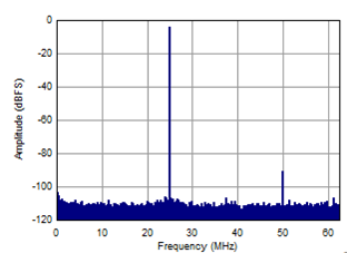
GUID-63AB996B-25CD-47DB-B346-EE4B00D62D1C-low.pngFigure 9-3 FFT for 100-MHz Input Signal
GUID-38CA2A51-1FD1-4511-BD53-8484C8094CF7-low.pngFigure 9-4 FFT for 270-MHz Input Signal