ZHCS116G May 2011 – December 2015 TPD4S014
PRODUCTION DATA.
- 1 特性
- 2 应用范围
- 3 说明
- 4 修订历史记录
- 5 Pin Configuration and Functions
- 6 Specifications
-
7 Detailed Description
- 7.1 Overview
- 7.2 Functional Block Diagram
- 7.3
Feature Description
- 7.3.1 Input Voltage Protection at VBUS up to 28 V DC
- 7.3.2 Low RON nFET Switch
- 7.3.3 ESD Performance D+/D-/ID/VBUS Pins
- 7.3.4 Overvoltage and Undervoltage Lockout Features
- 7.3.5 Capacitance TVS ESD Clamp for USB2.0 Hi-Speed Data Rate
- 7.3.6 Start-up Delay
- 7.3.7 OVP Glitch Immunity
- 7.3.8 Integrated Input Enable and Status Output Signal
- 7.3.9 Thermal Shutdown
- 7.4 Device Functional Modes
- 8 Application and Implementation
- 9 Power Supply Recommendations
- 10Layout
- 11器件和文档支持
- 12机械、封装和可订购信息
10 Layout
10.1 Layout Guidelines
- The optimum placement is as close to the connector as possible.
- EMI during an ESD event can couple from the trace being struck to other nearby unprotected traces, resulting in early system failures.
- The PCB designer needs to minimize the possibility of EMI coupling by keeping any unprotected traces away from the protected traces which are between the TVS and the connector.
- Keep traces between the connector and TPD4S014 on the same layer as TPD4S014.
- Route the protected traces as straight as possible.
- Eliminate any sharp corners on the protected traces between the TVS and the connector by using rounded corners with the largest radii possible.
- Electric fields tend to build up on corners, increasing EMI coupling.
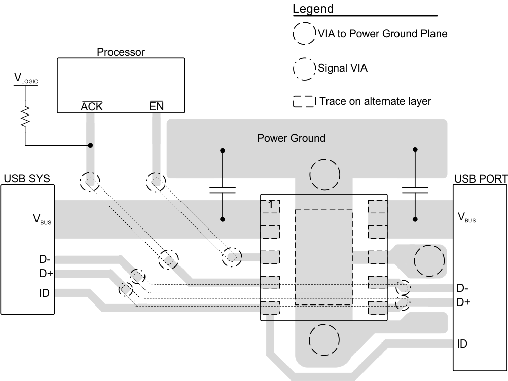
When designing layout for TPD4S014, note that VBUSOUT and VBUS pins allow for extra wide traces for good power delivery. In the example shown, these pins are routed with 25 mil (0.64 mm) wide traces. Place the VBUSOUT and VBUS capacitors as close to the device pins as possible. Pull ACK up to the Processor logic level high with a resistor. Use external and internal ground planes and stitch them together with VIAs as close to the GND pins of TPD4S014 as possible. This allows for a low impedance path to ground so that the device can properly dissipate any ESD events.
10.2 Layout Example
 Figure 17. Layout Recommendation