ZHCS158C July 2012 – January 2017 ADS1299 , ADS1299-4 , ADS1299-6
PRODUCTION DATA.
- 1 特性
- 2 应用
- 3 说明
- 4 修订历史记录
- 5 Device Comparison
- 6 Pin Configuration and Functions
- 7 Specifications
- 8 Parametric Measurement Information
-
9 Detailed Description
- 9.1 Overview
- 9.2 Functional Block Diagram
- 9.3
Feature Description
- 9.3.1 Analog Functionality
- 9.3.2
Digital Functionality
- 9.3.2.1 Digital Decimation Filter
- 9.3.2.2 Clock
- 9.3.2.3 GPIO
- 9.3.2.4 ECG and EEG Specific Features
- 9.4 Device Functional Modes
- 9.5
Programming
- 9.5.1 Data Format
- 9.5.2 SPI Interface
- 9.5.3
SPI Command Definitions
- 9.5.3.1 Sending Multi-Byte Commands
- 9.5.3.2 WAKEUP: Exit STANDBY Mode
- 9.5.3.3 STANDBY: Enter STANDBY Mode
- 9.5.3.4 RESET: Reset Registers to Default Values
- 9.5.3.5 START: Start Conversions
- 9.5.3.6 STOP: Stop Conversions
- 9.5.3.7 RDATAC: Read Data Continuous
- 9.5.3.8 SDATAC: Stop Read Data Continuous
- 9.5.3.9 RDATA: Read Data
- 9.5.3.10 RREG: Read From Register
- 9.5.3.11 WREG: Write to Register
- 9.6
Register Maps
- 9.6.1
User Register Description
- 9.6.1.1 ID: ID Control Register (address = 00h) (reset = xxh)
- 9.6.1.2 CONFIG1: Configuration Register 1 (address = 01h) (reset = 96h)
- 9.6.1.3 CONFIG2: Configuration Register 2 (address = 02h) (reset = C0h)
- 9.6.1.4 CONFIG3: Configuration Register 3 (address = 03h) (reset = 60h)
- 9.6.1.5 LOFF: Lead-Off Control Register (address = 04h) (reset = 00h)
- 9.6.1.6 CHnSET: Individual Channel Settings (n = 1 to 8) (address = 05h to 0Ch) (reset = 61h)
- 9.6.1.7 BIAS_SENSP: Bias Drive Positive Derivation Register (address = 0Dh) (reset = 00h)
- 9.6.1.8 BIAS_SENSN: Bias Drive Negative Derivation Register (address = 0Eh) (reset = 00h)
- 9.6.1.9 LOFF_SENSP: Positive Signal Lead-Off Detection Register (address = 0Fh) (reset = 00h)
- 9.6.1.10 LOFF_SENSN: Negative Signal Lead-Off Detection Register (address = 10h) (reset = 00h)
- 9.6.1.11 LOFF_FLIP: Lead-Off Flip Register (address = 11h) (reset = 00h)
- 9.6.1.12 LOFF_STATP: Lead-Off Positive Signal Status Register (address = 12h) (reset = 00h)
- 9.6.1.13 LOFF_STATN: Lead-Off Negative Signal Status Register (address = 13h) (reset = 00h)
- 9.6.1.14 GPIO: General-Purpose I/O Register (address = 14h) (reset = 0Fh)
- 9.6.1.15 MISC1: Miscellaneous 1 Register (address = 15h) (reset = 00h)
- 9.6.1.16 MISC2: Miscellaneous 2 (address = 16h) (reset = 00h)
- 9.6.1.17 CONFIG4: Configuration Register 4 (address = 17h) (reset = 00h)
- 9.6.1
User Register Description
- 10Applications and Implementation
- 11Power Supply Recommendations
- 12Layout
- 13器件和文档支持
- 14机械、封装和可订购信息
11 Power Supply Recommendations
The ADS1299-x has three power supplies: AVDD, AVDD1, and DVDD. For best performance, both AVDD and AVDD1 must be as quiet as possible. AVDD1 provides the supply to the charge pump block and has transients at fCLK. Therefore, star connect AVDD1 to the AVDD pins and AVSS1 to the AVSS pins. AVDD and AVDD1 noise that is nonsynchronous with the ADS1299-x operation must be eliminated. Bypass each device supply with 10-μF and 0.1-μF solid ceramic capacitors. For best performance, place the digital circuits (DSP, microcontrollers, FPGAs, and so forth) in the system so that the return currents on those devices do not cross the analog return path of the device. Power the ADS1299-x from unipolar or bipolar supplies.
Use surface-mount, low-cost, low-profile, multilayer ceramic-type capacitors for decoupling. In most cases, the VCAP1 capacitor is also a multilayer ceramic; however, in systems where the board is subjected to high- or low-frequency vibration, install a nonferroelectric capacitor, such as a tantalum or class 1 capacitor (C0G or NPO). EIA class 2 and class 3 dielectrics such as (X7R, X5R, X8R, and so forth) are ferroelectric. The piezoelectric property of these capacitors can appear as electrical noise coming from the capacitor. When using internal reference, noise on the VCAP1 node results in performance degradation.
11.1 Power-Up Sequencing
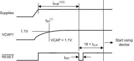
Before device power up, all digital and analog inputs must be low. At the time of power up, keep all of these signals low until the power supplies have stabilized, as shown in Figure 76.
Allow time for the supply voltages to reach their final value, and then begin supplying the master clock signal to the CLK pin. Wait for time tPOR, then transmit a reset pulse using either the RESET pin or RESET command to initialize the digital portion of the chip. Issue the reset after tPOR or after the VCAP1 voltage is greater than 1.1 V, whichever time is longer. Note that:
- tPOR is described in Table 30.
- The VCAP1 pin charge time is set by the RC time constant set by the capacitor value on VCAP1; see Figure 25.
After releasing the RESET pin, program the configuration registers. The power-up sequence timing is shown in Table 30.

Table 30. Timing Requirements for Figure 76
| MIN | MAX | UNIT | ||
|---|---|---|---|---|
| tPOR | Wait after power up until reset | 218 | tCLK | |
| tRST | Reset low duration | 2 | tCLK | |
11.2 Connecting the Device to Unipolar (5 V and 3.3 V) Supplies
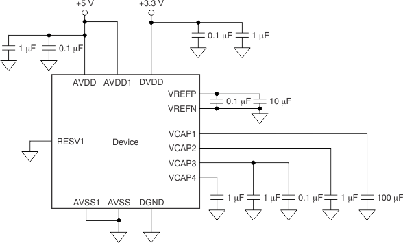
Figure 77 illustrates the ADS1299-x connected to a unipolar supply. In this example, analog supply (AVDD) is referenced to analog ground (AVSS) and digital supply (DVDD) is referenced to digital ground (DGND).

11.3 Connecting the Device to Bipolar (±2.5 V and 3.3 V) Supplies
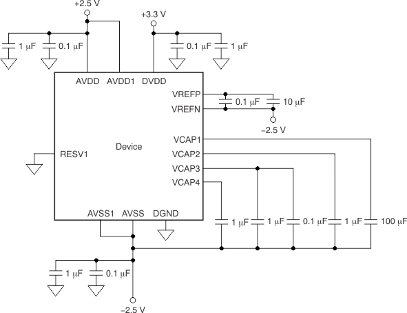
Figure 78 shows the ADS1299-x connected to a bipolar supply. In this example, the analog supplies connect to the device analog supply (AVDD). This supply is referenced to the device analog return (AVSS), and the digital supply (DVDD) is referenced to the device digital ground return (DGND).
