ZHCS158C July 2012 – January 2017 ADS1299 , ADS1299-4 , ADS1299-6
PRODUCTION DATA.
- 1 特性
- 2 应用
- 3 说明
- 4 修订历史记录
- 5 Device Comparison
- 6 Pin Configuration and Functions
- 7 Specifications
- 8 Parametric Measurement Information
-
9 Detailed Description
- 9.1 Overview
- 9.2 Functional Block Diagram
- 9.3
Feature Description
- 9.3.1 Analog Functionality
- 9.3.2
Digital Functionality
- 9.3.2.1 Digital Decimation Filter
- 9.3.2.2 Clock
- 9.3.2.3 GPIO
- 9.3.2.4 ECG and EEG Specific Features
- 9.4 Device Functional Modes
- 9.5
Programming
- 9.5.1 Data Format
- 9.5.2 SPI Interface
- 9.5.3
SPI Command Definitions
- 9.5.3.1 Sending Multi-Byte Commands
- 9.5.3.2 WAKEUP: Exit STANDBY Mode
- 9.5.3.3 STANDBY: Enter STANDBY Mode
- 9.5.3.4 RESET: Reset Registers to Default Values
- 9.5.3.5 START: Start Conversions
- 9.5.3.6 STOP: Stop Conversions
- 9.5.3.7 RDATAC: Read Data Continuous
- 9.5.3.8 SDATAC: Stop Read Data Continuous
- 9.5.3.9 RDATA: Read Data
- 9.5.3.10 RREG: Read From Register
- 9.5.3.11 WREG: Write to Register
- 9.6
Register Maps
- 9.6.1
User Register Description
- 9.6.1.1 ID: ID Control Register (address = 00h) (reset = xxh)
- 9.6.1.2 CONFIG1: Configuration Register 1 (address = 01h) (reset = 96h)
- 9.6.1.3 CONFIG2: Configuration Register 2 (address = 02h) (reset = C0h)
- 9.6.1.4 CONFIG3: Configuration Register 3 (address = 03h) (reset = 60h)
- 9.6.1.5 LOFF: Lead-Off Control Register (address = 04h) (reset = 00h)
- 9.6.1.6 CHnSET: Individual Channel Settings (n = 1 to 8) (address = 05h to 0Ch) (reset = 61h)
- 9.6.1.7 BIAS_SENSP: Bias Drive Positive Derivation Register (address = 0Dh) (reset = 00h)
- 9.6.1.8 BIAS_SENSN: Bias Drive Negative Derivation Register (address = 0Eh) (reset = 00h)
- 9.6.1.9 LOFF_SENSP: Positive Signal Lead-Off Detection Register (address = 0Fh) (reset = 00h)
- 9.6.1.10 LOFF_SENSN: Negative Signal Lead-Off Detection Register (address = 10h) (reset = 00h)
- 9.6.1.11 LOFF_FLIP: Lead-Off Flip Register (address = 11h) (reset = 00h)
- 9.6.1.12 LOFF_STATP: Lead-Off Positive Signal Status Register (address = 12h) (reset = 00h)
- 9.6.1.13 LOFF_STATN: Lead-Off Negative Signal Status Register (address = 13h) (reset = 00h)
- 9.6.1.14 GPIO: General-Purpose I/O Register (address = 14h) (reset = 0Fh)
- 9.6.1.15 MISC1: Miscellaneous 1 Register (address = 15h) (reset = 00h)
- 9.6.1.16 MISC2: Miscellaneous 2 (address = 16h) (reset = 00h)
- 9.6.1.17 CONFIG4: Configuration Register 4 (address = 17h) (reset = 00h)
- 9.6.1
User Register Description
- 10Applications and Implementation
- 11Power Supply Recommendations
- 12Layout
- 13器件和文档支持
- 14机械、封装和可订购信息
12 Layout
12.1 Layout Guidelines
TI recommends employing best design practices when laying out a printed-circuit board (PCB) for both analog and digital components. This recommendation generally means that the layout separates analog components [such as ADCs, amplifiers, references, digital-to-analog converters (DACs), and analog MUXs] from digital components [such as microcontrollers, complex programmable logic devices (CPLDs), field-programmable gate arrays (FPGAs), radio frequency (RF) transceivers, universal serial bus (USB) transceivers, and switching regulators]. An example of good component placement is shown in Figure 79. Although Figure 79 provides a good example of component placement, the best placement for each application is unique to the geometries, components, and PCB fabrication capabilities employed. That is, there is no single layout that is perfect for every design and careful consideration must always be used when designing with any analog component.
 Figure 79. System Component Placement
The following outlines some basic recommendations for the layout of the ADS1299-x to get the best possible performance of the ADC. A good design can be ruined with a bad circuit layout.
- Separate analog and digital signals. To start, partition the board into analog and digital sections where the layout permits. Route digital lines away from analog lines. This configuration prevents digital noise from coupling back into analog signals.
- The ground plane can be split into an analog plane (AGND) and digital plane (DGND), but is not necessary. Place digital signals over the digital plane, and analog signals over the analog plane. As a final step in the layout, the split between the analog and digital grounds must be connected together at the ADC.
- Fill void areas on signal layers with ground fill.
- Provide good ground return paths. Signal return currents flow on the path of least impedance. If the ground plane is cut or has other traces that block the current from flowing right next to the signal trace, then the current must find another path to return to the source and complete the circuit. If current is forced into a longer path, the chances that the signal radiates increases. Sensitive signals are more susceptible to EMI interference.
- Use bypass capacitors on supplies to reduce high-frequency noise. Do not place vias between bypass capacitors and the active device. Placing the bypass capacitors on the same layer as close to the active device yields the best results.
- Analog inputs with differential connections must have a capacitor placed differentially across the inputs. The differential capacitors must be of high quality. The best ceramic chip capacitors are C0G (NPO), which have stable properties and low noise characteristics.
12.2 Layout Example
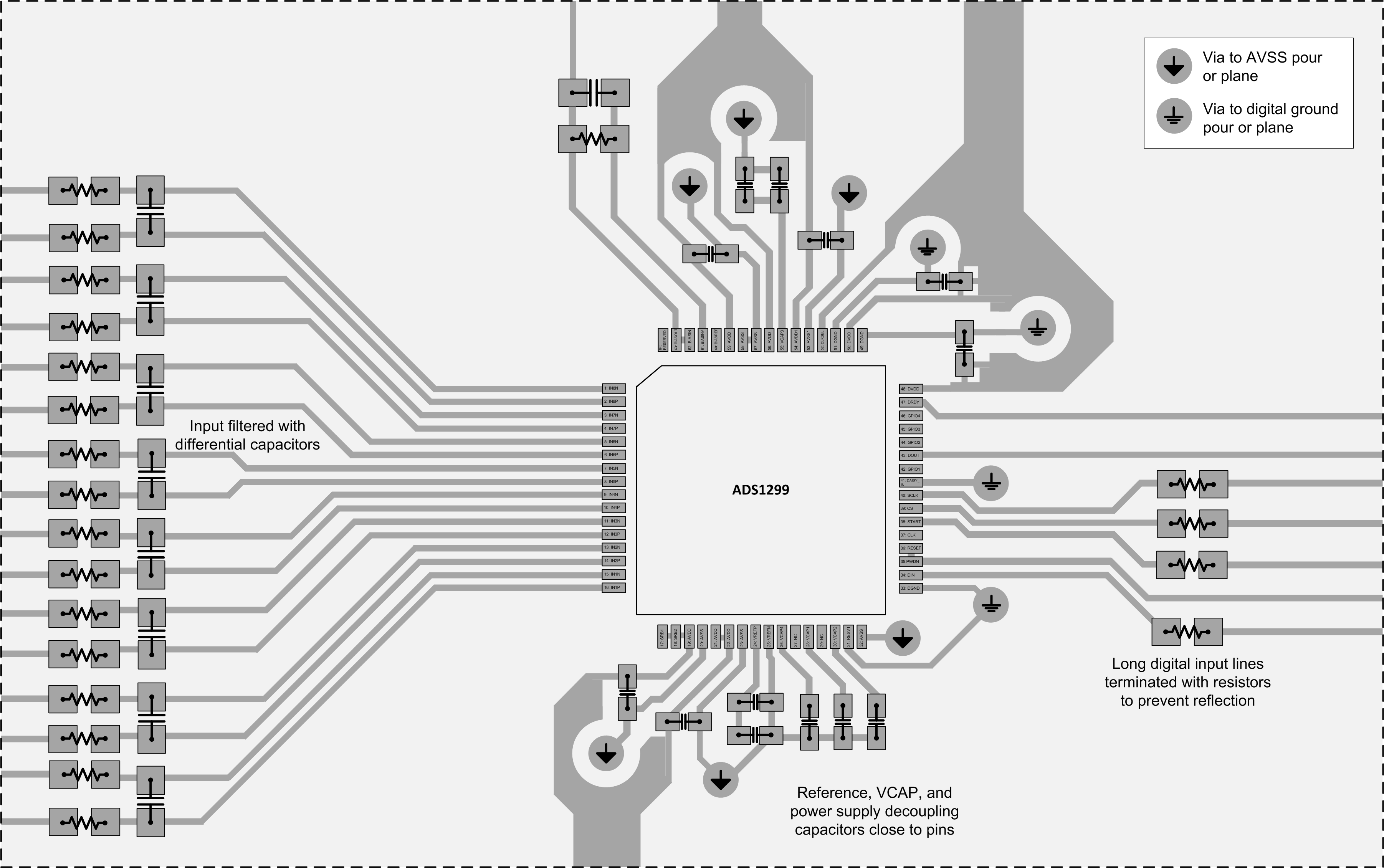
Figure 80 is an example layout of the ADS1299 requiring a minimum of two PCB layers. The example circuit is shown for either a single analog supply or a bipolar-supply connection. In this example, polygon pours are used as supply connections around the device. If a three- or four-layer PCB is used, the additional inner layers can be dedicated to route power traces. The PCB is partitioned with analog signals routed from the left, digital signals routed to the right, and power routed above and below the device.
 Figure 80. ADS1299 Example Layout