ZHCS163C August 2011 – February 2016 ADS8528 , ADS8548 , ADS8568
PRODUCTION DATA.
- 1 特性
- 2 应用
- 3 说明
- 4 修订历史记录
- 5 Device Comparison Table
- 6 Pin Configuration and Functions
-
7 Specifications
- 7.1 Absolute Maximum Ratings
- 7.2 ESD Ratings
- 7.3 Recommended Operating Conditions
- 7.4 Thermal Information
- 7.5 Electrical Characteristics: General
- 7.6 Electrical Characteristics: ADS8528
- 7.7 Electrical Characteristics: ADS8548
- 7.8 Electrical Characteristics: ADS8568
- 7.9 Serial Interface Timing Requirements
- 7.10 Parallel Interface Timing Requirements (Read Access)
- 7.11 Parallel Interface Timing Requirements (Write Access)
- 7.12 Typical Characteristics
- 8 Parameter Measurement information
- 9 Detailed Description
- 10Application and Implementation
- 11Power Supply Recommendations
- 12Layout
- 13器件和文档支持
- 14机械、封装和可订购信息
9 Detailed Description
9.1 Overview
The ADS85x8 series includes eight 12-, 14-, and 16-bit analog-to-digital converters (ADCs) that operate based on the successive approximation register (SAR) architecture. This architecture is designed on the charge redistribution principle that inherently includes a sample-and-hold function. The eight analog inputs are grouped into four channel pairs. These channel pairs can be sampled and converted simultaneously, preserving the relative phase information of the signals of each pair. Separate conversion start signals allow simultaneous sampling on each channel pair of four, six, or eight channels. These devices accept single-ended, bipolar analog input signals in the selectable ranges of ±4 VREF or ±2 VREF with an absolute value of up to ±12 V; see the Analog Inputs section.
The devices offer an internal 2.5-V or 3-V reference source followed by a 10-bit digital-to-analog converter (DAC) that allows the reference voltage VREF to be adjusted in 2.44-mV or 2.93-mV steps, respectively.
The ADS85x8 also offer a selectable parallel or serial interface that can be used in hardware or software mode; see the Device Configuration section for details. The Analog and Digital sections describe the functionality and control of the device in detail.
9.2 Functional Block Diagram
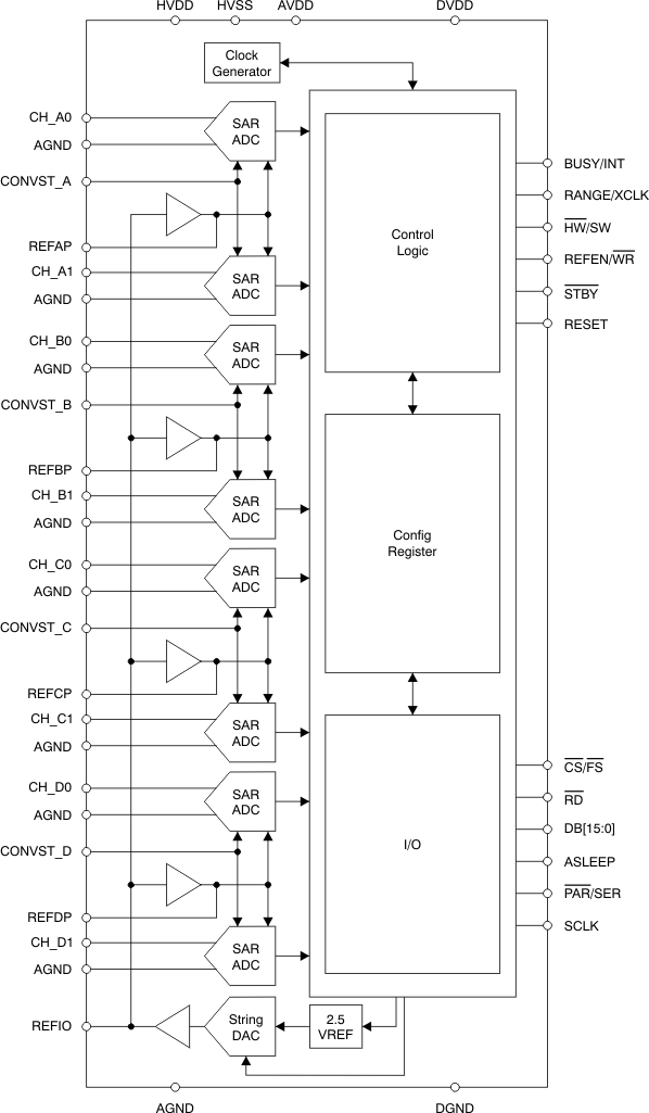
9.3 Feature Description
9.3.1 Analog
This section addresses the analog input circuit, the ADCs and control signals, and the reference design of the device.
9.3.1.1 Analog Inputs
The inputs and the converters are of single-ended bipolar type. The absolute voltage range can be selected using the RANGE pin (in hardware mode) or RANGE_x bits (in software mode) in the Configuration (CONFIG) register to either ±4 VREF or ±2 VREF. With the internal reference set to 2.5 V (VREF bit C13 = 0 in the CONFIG register), the input voltage range can be ±10 V or ±5 V. With the internal reference source set to 3 V (CONFIG bit C13 = 1), an input voltage range of ±12 V or ±6 V can be configured. The logic state of the RANGE pin is latched with the falling edge of BUSY (if CONFIG bit C26 = 0).
The input current on the analog inputs depends on the actual sample rate, input voltage, and signal source impedance. Essentially, the current into the analog inputs charges the internal capacitor array only during the sampling period (tACQ). The source of the analog input voltage must be able to charge the input capacitance of 10 pF in ±4-VREF mode or of 20 pF in ±2-VREF mode to a 12-, 14-, or 16-bit accuracy level within the acquisition time; see Figure 35. During the conversion period, there is no further input current flow and the input impedance is greater than 1 MΩ. To ensure a defined start condition, the sampling capacitors of the ADS85x8 are pre-charged to a fixed internal voltage before switching into sampling mode.
To maintain the linearity of the converter, the inputs must always remain within the specified range defined in the Electrical Characteristics table. The minimum –3-dB bandwidth of the driving operational amplifier can be calculated using Equation 1:

where
- n = 12, 14, or 16; n is the resolution of the ADS85x8
With a minimum acquisition time of tACQ = 280 ns, the required minimum bandwidth of the driving amplifier is 5.2 MHz for the ADS8528, 6.0 MHz for the ADS8548, or 6.7 MHz for the ADS8568. The required bandwidth can be lower if the application allows a longer acquisition time. A gain error occurs if a given application does not fulfill the bandwidth requirement shown in Equation 1.
A driving operational amplifier may not be required if the impedance of the signal source (RSOURCE) fulfills the requirement of Equation 2:

where
- n = 12, 14, or 16; n is the resolution of the ADC
- CS = 10 pF is the sample capacitor value in VIN = ±4-VREF mode
- RSER = 200 Ω is the input resistor value
- and RSW = 130 Ω is the switch resistance value
With a minimum acquisition time of tACQ = 280 ns, the maximum source impedance must be less than 2.7 kΩ for the ADS8528, 2.3 kΩ for the ADS8548, and 2.0 kΩ for the ADS8568 in ±4V-REF mode, or less than 1.2 kΩ for the ADS8528, 1.0 kΩ for the ADS8548, and 0.8 kΩ for the ADS8568 in ±2-VREF mode. The source impedance can be higher if the application allows a longer acquisition time.
9.3.1.2 Analog-to-Digital Converter (ADC)
The device includes eight ADCs that operate with either an internal or an external conversion clock.
9.3.1.3 Conversion Clock
The device uses either an internally-generated (CCLK) or an external (XCLK) conversion clock signal (in software mode only). In default mode, the device generates an internal clock. In this case, a complete conversion including the pre-charging of the sample capacitors takes 19 to 20 clock cycles, depending on the setup time of the incoming CONVST_x signal with relation to the CCLK rising edge.
When the CLKSEL bit is set high (CONFIG bit C29), an external conversion clock can be applied on pin 34. A complete conversion process requires 19 clock cycles in this case if the tSCVX timing requirement is fulfilled. The external clock can remain low between conversions.
If the application requires lowest power dissipation at low data rates, using the auto-sleep mode activated with pin 36 (ASLEEP) is recommended. In this case, a conversion cycle takes up to 26 clock cycles (see the Reset and Power-Down Modes section for more details).
9.3.1.4 CONVST_x
The analog inputs of each channel pair (CH_x0, CH_x1) are held with the rising edge of the corresponding CONVST_x signal. The conversion automatically starts with the next rising edge of the conversion clock. CONVST_A is a master conversion start that resets the internal state machine and causes the data output to start with the result of channel A0. In cases where channel pairs of the device are used at different data rates, CONVST_A must always be the one used at the highest frequency.
A conversion start must not be issued during an ongoing conversion on the corresponding channel pair. However, conversions are allowed to be initiated on other input pairs; see the Sequential Operation section for more details.
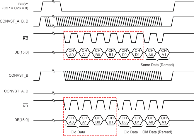
If a parallel interface is used, the content of the output port depends on which CONVST_x signals are issued. Figure 36 shows examples of different scenarios with all channel pairs active.
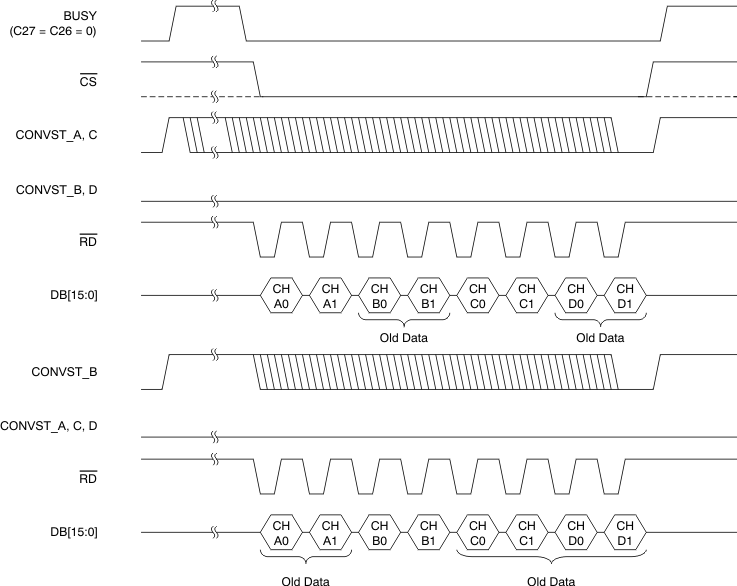 Figure 36. Data Output versus CONVST_x (All Channels Active)
9.3.1.5 Data Readout and BUSY/INT Signal
The BUSY signal indicates if a conversion is in progress. The BUSY signal goes high with a rising edge of any CONVST_x signal and returns low again when the last channel pair completes the conversion cycle.
When operating the device with an external clock (CONFIG bit 29, CLKSEL = 1), data readout can be initiated immediately after the falling edge of the BUSY signal or after 19 complete conversion clock cycles (XCLK), respectively.
When using the device with an internal conversion clock (CONFIG bit 29, CLKSEL = 0), data can be retrieved after tCONV(max) independently from the BUSY signal. In case the data readout is referred to the falling edge of the BUSY signal, the readout sequence cannot start before tBUFS/BUCS after the falling edge, corresponding to 1 CCLK cycle (for example, 86 ns for the ADS8568).
In contrast, the INT signal goes high when a new conversion result is loaded in the output register (which occurs when the conversion completes) and remains high until the next read access, as shown in Figure 37.
The polarity of the BUSY/INT signal can be changed using CONFIG bit C26. The mode of pin 35 can be controlled using CONFIG bit C27.
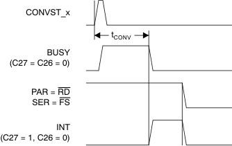 Figure 37. BUSY versus INT Behavior of Pin 35
9.3.1.6 Sequential Operation
The four channel pairs of the ADS8528, ADS8548, and ADS8568 can run in sequential mode, with the corresponding CONVST_x signals interleaved. In this case, the BUSY output transitions low for a single conversion clock cycle (tCCLK) whenever a channel pair completes a conversion. BUSY finally remains low when the conversion of the last channel pair completes. Figure 38 shows the behavior of the BUSY output in this mode.
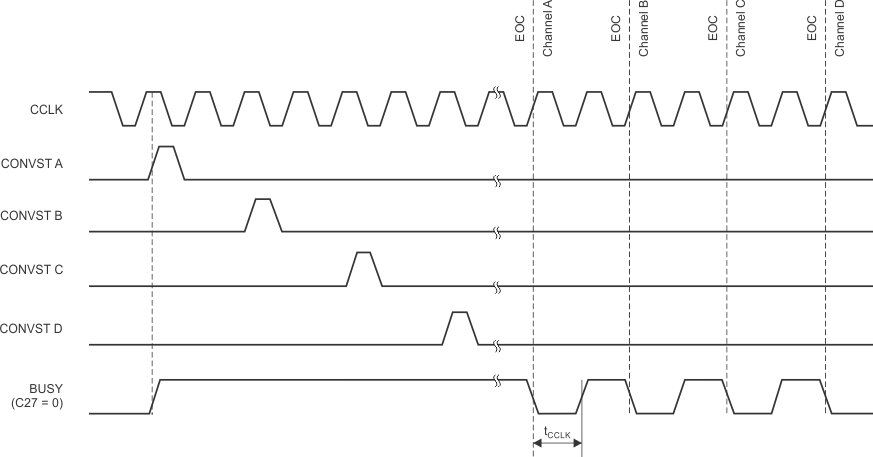
NOTE:
EOC = end of conversion (internal signal).For best performance, operation with an external clock is recommended (CONFIG bit 29, CLKSEL = 1). Initiate each conversion start during the high phase of the external clock; see Figure 40.
The time between two CONVST_x pulses must be at least one conversion clock cycle. In case the skew of the CONVST_x signals is less than one conversion clock cycle, the data readout cannot be started before tCCLK after the falling edge of the BUSY signal.
9.3.1.7 Reference
The ADS85x8 provides an internal, low-drift, 2.5-V reference source. To increase the input voltage range, the reference voltage can be switched to 3-V mode using the VREF bit (CONFIG bit C13). The reference feeds a 10-bit string-DAC controlled by the REFDAC[9:0] bits in the Configuration (CONFIG) register. The buffered DAC output is connected to the REFIO pin. In this way, the voltage at this pin is programmable in 2.44-mV steps (2.92 mV in 3-V mode) and adjustable to the applications needs without additional external components. The actual output voltage can be calculated using Equation 3:

where
- Range = the chosen maximum reference voltage output range (2.5 V or 3 V)
- Code = the decimal value of the DAC register content
Table 1 lists some examples of internal reference DAC settings with a reference range set to 2.5 V. However, to ensure proper performance, the DAC output voltage must not be programmed below 0.5 V.
Decouple the buffered output of the DAC with a 100-nF capacitor (minimum); for best performance, a 470-nF capacitor is recommended. If the internal reference is placed into power-down (default), an external reference voltage can drive the REFIO pin.
Table 1. DAC Settings Examples (2.5-V Operation)
| VREFOUT | DECIMAL CODE | BINARY CODE | HEXADECIMAL CODE |
|---|---|---|---|
| 0.5 V | 204 | 00 1100 1100 | CCh |
| 1.25 V | 511 | 01 1111 1111 | 1FFh |
| 2.5 V | 1023 | 11 1111 1111 | 3FFh |
The voltage at the REFIO pin is buffered with four internal amplifiers, one for each ADC pair. The output of each buffer must be decoupled with a 10-µF capacitor between the pin pairs of 3 and 6, 43 and 46, 50 and 53, and 60 and 63. The 10-µF capacitors are available as ceramic 0805-SMD components and in X5R quality.
The internal reference buffers can be powered down to decrease the power dissipation of the device. In this case, external reference drivers can be connected to the REFAP, REFBP, REFCP, and REFDP pins. With 10-µF decoupling capacitors, the minimum required bandwidth can be calculated using Equation 4:

With the minimum tCONV of 1.33 µs, the external reference buffers require a minimum bandwidth of 83 kHz.
9.3.2 Digital
This section describes the digital control and the timing of the device in detail.
9.3.2.1 Device Configuration
Depending on the desired mode of operation, the ADS85x8 can be configured using the external pins or the Configuration register (CONFIG), as shown in Table 2.
Table 2. ADS85x8 Configuration Settings
| INTERFACE MODE | HARDWARE MODE (HW/SW = 0) | SOFTWARE MODE (HW/SW = 1) |
|---|---|---|
| Parallel (PAR/SER = 0) | Configuration using pins and (optionally) Configuration register bits C30, C29, C[27:26], C22, C20, C18, C14, C13, and C[9:0] | Configuration using Configuration register bits C[31:0] only; status of pins 9, 11, 20, and 34 are disregarded (if C29 = C28 = 0) |
| Serial (PAR/SER = 1) | Configuration using pins and (optionally) Configuration register bits C30, C29, C[27:26], C22, C20, C18, C13, and C[9:0] | Configuration using Configuration register bits C[31:0] only; status of pins 9, 11, 20, and 34 are disregarded (if C29 = C28 = 0) |
9.3.2.2 Parallel Interface
To use the device with the parallel interface, hold the PAR/SER pin low. The maximum achievable data throughput rate is 650 kSPS for the ADS8528, 600 kSPS for the ADS8548, and 510 kSPS for the ADS8568 in this case.
Access to the ADS85x8 is controlled as illustrated in Figure 2 and Figure 3.
9.3.2.3 Serial Interface
The serial interface mode is selected by setting the PAR/SER pin high. In this case, each data transfer starts with the falling edge of the frame synchronization input (FS). The conversion results are presented on the serial data output pins SDO_A (always active), SDO_B, SDO_C, and SDO_D, depending on the selections made using the SEL_xx pins. Starting with the most significant bit (MSB), the output data are changed with the SCLK falling edge. The ADS8528 and ADS8548 output data maintain the LSB-aligned, 16-bit format with leading bits containing the extended sign (see Table 3). Serial data input SDI are latched with the SCLK falling edge.
The serial interface can be used with one, two, or four output ports. Port SDO_B can be enabled using pin 27 (SEL_B) and ports SDO_C and SDO_D are enabled using pin 28 (SEL_CD). If all four serial data output ports are selected, data can be read with either two 16-bit data transfers or with a single 32-bit data transfer. The data of channels CH_x0 are available first, followed by data from channels CH_x1. The maximum achievable data throughput rate is 480 kSPS for the ADS8528, 450 kSPS for the ADS8548, and 400 kSPS for the ADS8568 in this case.
If the application allows a data transfer using two ports only, the SDO_A and SDO_B outputs are used. The device outputs data from channel CH_A0 followed by CH_A1, CH_C0, and CH_C1 on SDO_A; data from channel CH_B0 followed by CH_B1, CH_D0, and CH_D1 occur on SDO_B. In this case, a data transfer of four 16-bit words, two 32-bit words, or one continuous 64-bit word is supported. The maximum achievable data throughput rate is 360 kSPS for the ADS8528, 345 kSPS for the ADS8548, and 315 kSPS for the ADS8568 in this case.
The output SDO_A is always active and exclusively used if only one serial data port is used in the application. Data are available in the following order: CH_A0, CH_A1, CH_B0, CH_B1, CH_C0, CH_C1, CH_D0, and CH_D1. Data can be read using eight 16-bit transfers, four 32-bit transfers, two 64-bit transfers, or a single 128-bit transfer. The maximum achievable data throughput rate is 235 kSPS for the ADS8528, 230 kSPS for the ADS8548 and 215 kSPS for the ADS8568 in this case. Figure 1 and Figure 39 illustrate all possible scenarios in more detail.
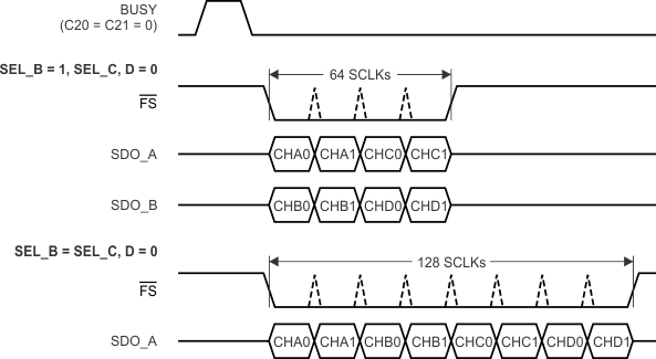 Figure 39. Data Output with One or Two Active SDOs (All Input Channels Active and Converted)
9.3.2.4 Output Data Format
The data output format of the ADS85x8 is binary twos complement, as shown in Table 3. For the ADS8528 and ADS8548 (that deliver 12-bit or 14-bit conversion results, respectively), the leading bits of either the 16-bit frame (serial interface) or the output pins (DB[15:12] for the ADS8528 or DB[15:14] for the ADS8548 in parallel mode) deliver a sign extension.
Table 3. Output Data Format
| DESCRIPTION | INPUT VOLTAGE VALUE | BINARY CODE HEXADECIMAL CODE | ||
|---|---|---|---|---|
| ADS8528 | ADSS8548 | ADS8568 | ||
| Positive full-scale | 4 VREF or 2 VREF | 0000 0111 1111 1111 07FFh | 0001 1111 1111 1111 1FFFh | 0111 1111 1111 1111 7FFFh |
| Midscale 0.5 LSB | VREF / (2 × resolution) | 0000 0000 0000 0000 0000h | 0000 0000 0000 0000 0000h | 0000 0000 0000 0000 0000h |
| Midscale –0.5 LSB | –VREF / (2 × resolution) | 1111 1111 1111 1111 FFFFh | 1111 1111 1111 1111 FFFFh | 1111 1111 1111 1111 FFFFh |
| Negative full-scale | –4 VREF or –2 VREF | 1111 1000 0000 0000 F800h | 1110 0000 0000 0000 E000h | 1000 0000 0000 0000 8000h |
9.4 Device Functional Modes
9.4.1 Hardware Mode
With the HW/SW input (pin 41) set low, the device functions are controlled via the pins and, optionally, Configuration register bits C30, C29, C[27:26], C22, C20, C18, C14 (in parallel interface mode only), C13, and C[9:0].
The device can generally be used in hardware mode but can be switched to software mode to initialize or adjust the Configuration register settings (for example, the internal reference DAC) and back to hardware mode thereafter.
9.4.2 Software Mode
When the HW/SW input is set high, the device operates in software mode with functionality set only by the Configuration register bits (corresponding pin settings are ignored).
If the parallel interface is used, an update of all Configuration register settings is performed by issuing two 16-bit write accesses on pins DB[15:0] (to avoid losing data, the entire sequence must be finished before starting a new conversion). Do not hold CS low during these two accesses. To enable the actual update of the register settings, the first bit (C31) must be set to 1 during the access.
If the serial interface is used, the update of the register contents can be performed continuously (combined read/write access). Optionally, to reduce the data transfer on the SDI line and the electromagnetic interference (EMI) of the system, the SDI input can be pulled low when a register update is not required. Figure 40 illustrates the different Configuration register update options.
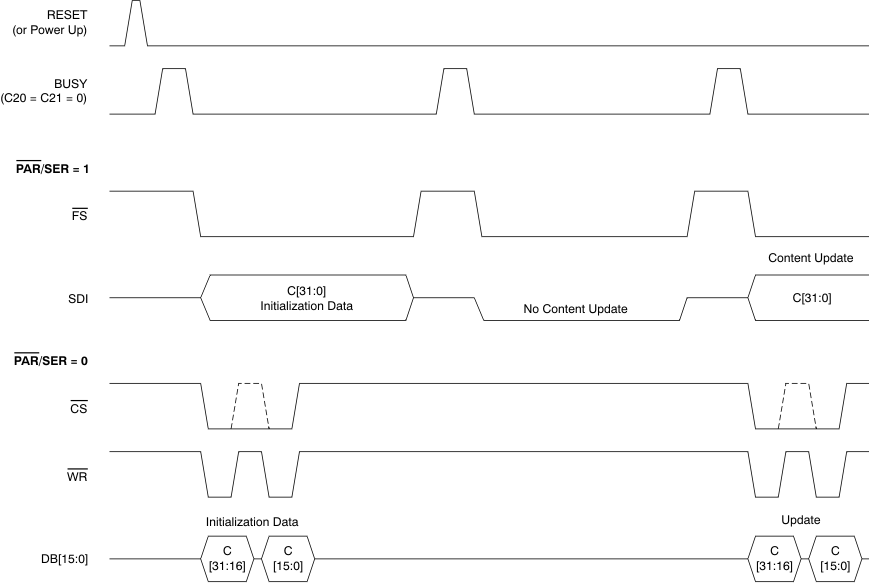 Figure 40. Configuration Register Update Options
9.4.3 Daisy-Chain Mode
The serial interface of the ADS85x8 supports a daisy-chain feature that allows cascading of multiple devices to minimize the board space requirements and simplify routing of the data and control lines. In this case, the DB3/DCIN_A, DB2/DCIN_B, DB1/DCIN_C, and DB0/DCIN_D pins are used as serial data inputs for channels A, B, C, and D, respectively. Figure 41 shows an example of a daisy-chain connection of three devices sharing a common CONVST line to allow simultaneous sampling of 24 analog channels along with the corresponding timing diagram.
To activate the daisy-chain mode, the DCEN pin must be pulled high. However, the DCEN of the first device in the chain must remain low.
In applications where not all channel pairs are used, declaring the device with disabled channel pairs to be the first in the daisy-chain is recommended.
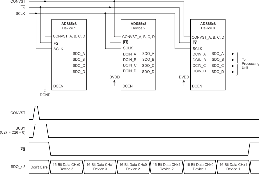 Figure 41. Example of Daisy-Chaining Three Devices
9.4.4 Reset and Power-Down Modes
The device supports two reset mechanisms: a power-on reset (POR) and a pin-controlled reset (RESET) that can be issued using pin 10. Both the POR and RESET function as a master reset that causes any ongoing conversion to be interrupted, the Configuration register content to be set to the default value, and all channels to be switched into sample mode.
When the device is powered up, POR sets the device in default mode when AVDD reaches 1.2 V. In normal operation, glitches on the AVDD supply below this threshold trigger a device reset.
The entire device, except for the digital interface, can be powered down by pulling the STBY pin low (pin 9). Data can be retrieved when in standby mode because the digital interface section remains active. To power the device on again, the STBY pin must be brought high. The device is ready to start a new conversion after the 10 ms required to activate and settle the internal circuitry. This user-controlled approach can be used in applications that require lower data throughput rates at lowest power dissipation. The content of CONFIG is not changed during standby mode and is not required to perform a reset after returning to normal operation.
Although standby mode affects the entire device, each device channel pair (except channel pair A, which is the master channel pair and is always active) can also be individually switched off by setting the Configuration register bits C22, C20, and C18 (PD_x). If a certain channel pair is powered-down in this manner, the output register is disabled as shown in Figure 42. When reactivated, the relevant channel pair requires 10 ms to fully settle before starting a new conversion.
NOTE:
Boxed areas indicate the minimum required frame to acquire all new conversion results. The read access can be interrupted, thereafter.Auto-sleep mode is enabled by pulling pin 36 (ASLEEP) high. If auto-sleep mode is enabled, the ADS85x8 automatically reduce the current requirement to 7 mA (IAVDD) after finishing a conversion; thus, the end of conversion actually activates this power-down mode. Triggering a new conversion by applying a positive CONVST_x edge starts the wake-up sequence to put the device back into normal operation. At the beginning, all required building blocks power-up and the sampling switches close again. This sequence takes six to seven conversion clock cycles of either the internal or external clock. During this time, the sampling capacitance must be recharged to the input signal with the required 12-bit, 14-bit, or 16-bit accuracy level. The bandwidth requirements of the driving operational amplifier described in the Analog Inputs section must be fulfilled. At the end of the sequence, the new sample is taken and the conversion starts automatically, as shown in Figure 43. Therefore, a complete conversion process takes 25 to 26 conversion clock cycles; thus, the maximum throughput rate in auto-sleep mode is reduced to a maximum of 400 kSPS for the ADS8528, 375 kSPS for the ADS8548, and 330 kSPS for the ADS8568 in serial interface mode. In parallel mode, the maximum data rates are 510 kSPS for the ADS8528, 470 kSPS for the ADS8548, and 400 kSPS for the ADS8568. If enabled, the internal reference remains active during auto-sleep mode. Table 4 compares the analog current requirements of the device in different modes.
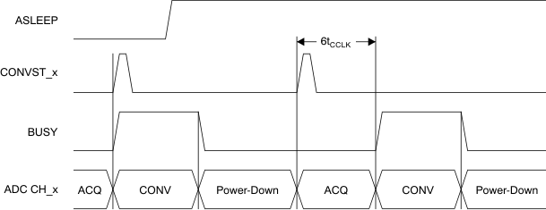 Figure 43. Auto-Sleep Power-Down Mode
Table 4. Maximum Analog Current (IAVDD) Demand of the ADS85x8
| OPERATIONAL MODE | ANALOG CURRENT (IAVDD) | ENABLED, DISABLED BY | ACTIVATED BY | NORMAL OPERATION TO POWER-DOWN DELAY | RESUMED BY | POWER-UP TO NORMAL OPERATION DELAY | POWER-UP TO NEXT CONVERSION START TIME |
|---|---|---|---|---|---|---|---|
| Normal operation | 12.5 mA/ch pair at maximum data rate | Power on | CONVST_x | — | — | — | — |
| Power off | |||||||
| Auto-sleep | 1.75 mA/ch pair | ASLEEP = 1 | Each end of conversion | At BUSY falling edge | CONVST_x | Immediate | 7 × tCCLK max |
| ASLEEP = 0 | |||||||
| Power-down of channel pair X | 16 µA (channel pair X) |
HW/SW = 1 | PD_x = 1 (CONFIG bit) | Immediate | PD_x = 0 (CONFIG bit) | Immediate after completing CONFIG update | 10 ms |
| HW/SW = 0 | |||||||
| Power-down (entire device) | 30 µA | Power on | STBY = 0 | Immediate | STBY = 1 | Immediate | 10 ms |
| Power off |
9.5 Register Maps
9.5.1 Configuration (CONFIG) Register
The Configuration register settings can only be changed in software mode and are not affected when switching to hardware mode thereafter. The register values are independent from input pin settings. Changes are active with the second WR rising edge in parallel interface mode or with the 32nd SCLK falling edge of the access where the register content is updated in serial mode. The CONFIG content is defined in CONFIG: Configuration Register (default = 000003FFh).
9.5.1.1 CONFIG: Configuration Register (default = 000003FFh)
| 31 | 30 | 29 | 28 | 27 | 26 | 25 | 24 |
| WRITE_EN | READ_EN | CLKSEL | CLKOUT | BUSY/INT | BUSY POL | STBY | RANGE_A |
| 23 | 22 | 21 | 20 | 19 | 18 | 17 | 16 |
| RANGE_B | PD_B | RANGE_C | PD_C | RANGE_D | PD_D | Don't care | Don't care |
| 15 | 14 | 13 | 12 | 11 | 10 | 9 | 8 |
| REFEN | REFBUF | VREF | Don't care | Don't care | Don't care | D9 | D8 |
| 7 | 6 | 5 | 4 | 3 | 2 | 1 | 0 |
| D7 | D6 | D5 | D4 | D3 | D2 | D1 | D0 |
| Bit 31 | WRITE_EN: Register update enable |
| This bit is not active in hardware mode. 0 = Register content update disabled (default) 1 = Register content update enabled |
|
| Bit 30 | READ_EN: Register read-out access enable |
| This bit is not active in hardware mode. 0 = Normal operation (conversion results available on SDO_A) 1 = Configuration register contents output on SDO_A with next two accesses (READ_EN automatically resets to 0 thereafter) |
|
| Bit 29 | CLKSEL: Conversion clock selector |
| This bit is active in hardware mode. 0 = Normal operation with internal conversion clock; mandatory in hardware mode (default) 1 = External conversion clock applied through pin 34 (XCLK) is used (conversion takes 19 clock cycles) |
|
| Bit 28 | CLKOUT: Internal conversion clock output enable |
| This bit is not active in hardware mode. 0 = Normal operation (default) 1 = Internal conversion clock is available at pin 34 |
|
| Bit 27 | BUSY/INT: Busy/interrupt selector |
| This bit is active in hardware mode. 0 = BUSY/INT pin is in BUSY mode (default) 1 = BUSY/INT pin is in interrupt mode (INT); can only be used if all eight channels are sampled simultaneously (all CONVST_x tied together) |
|
| Bit 26 | BUSY POL: BUSY/INT polarity selector |
| This bit is active in hardware mode. 0 = BUSY/INT active high (default) 1 = BUSY/INT active low |
|
| Bit 25 | STBY: Power-down enable |
| This bit is not active in hardware mode. 0 = Normal operation (default) 1 = Entire device is powered down (including the internal clock and reference) |
|
| Bit 24 | RANGE_A: Input voltage range selector for channel pair A |
| This bit is not active in hardware mode. 0 = Input voltage range: 4 VREF (default) 1 = Input voltage range: 2 VREF |
|
| Bit 23 | RANGE_B: Input voltage range selector for channel pair B |
| This bit is not active in hardware mode. 0 = Input voltage range: 4 VREF (default) 1 = Input voltage range: 2 VREF |
|
| Bit 22 | PD_B: Power-down enable for channel pair B |
| This bit is active in hardware mode. 0 = Normal operation (default) 1 = Channel pair B is powered down |
|
| Bit 21 | RANGE_C: Input voltage range selector for channel pair C |
| This bit is not active in hardware mode. 0 = Input voltage range: 4 VREF (default) 1 = Input voltage range: 2 VREF |
|
| Bit 20 | PD_C: Power-down enable for channel pair C |
| This bit is active in hardware mode. 0 = Normal operation (default) 1 = Channel pair C is powered down |
|
| Bit 19 | RANGE_D: Input voltage range selector for channel pair D |
| This bit is not active in hardware mode. 0 = Input voltage range: 4 VREF (default) 1 = Input voltage range: 2 VREF |
|
| Bit 18 | PD_D: Power-down enable for channel pair D |
| This bit is active in hardware mode. 0 = Normal operation (default) 1 = Channel pair D is powered down |
|
| Bits 17-16 | Not used (default = 0) |
| Bit 15 | REF_EN: Internal reference enable |
| This bit is not active in hardware mode. 0 = Internal reference source disabled (default) 1 = Internal reference source enabled |
|
| Bit 14 | REFBUF: Internal reference buffers disable |
| This bit is active in hardware mode if the parallel interface is used. 0 = Internal reference buffers enabled (default) 1 = Internal reference buffers disabled |
|
| Bit 13 | VREF: Internal reference voltage selector |
| This bit is active in hardware mode. 0 = Internal reference voltage set to 2.5 V (default) 1 = Internal reference voltage set to 3.0 V |
|
| Bits 12-10 | Not used (default = 0) |
| Bits 9-0 | D[9:0]: REFDAC setting bits |
| These bits are active in hardware mode. These bits correspond to the settings of the internal reference DACs (compare to the Reference section). Bit 9 is the MSB of the DAC. Default value is 3FFh (2.5 V, typ). |