ZHCS234B August 2012 – January 2016 PCM5141 , PCM5142
PRODUCTION DATA.
- 1 特性
- 2 应用
- 3 说明
- 4 修订历史记录
- 5 Device Comparison
- 6 Pin Configuration and Functions
-
7 Specifications
- 7.1 Absolute Maximum Ratings
- 7.2 ESD Ratings
- 7.3 Recommended Operating Conditions
- 7.4 Thermal Information
- 7.5 Electrical Characteristics
- 7.6 Timing Requirements: SCK Input
- 7.7 Timing Requirements: PCM Audio Data
- 7.8 Timing Requirements: I2S Master
- 7.9 Timing Requirements: XSMT
- 7.10 Switching Characteristics
- 7.11 Typical Characteristics
-
8 Detailed Description
- 8.1 Overview
- 8.2 Functional Block Diagram
- 8.3
Feature Description
- 8.3.1 Terminology
- 8.3.2 Audio Data Interface
- 8.3.3 XSMT Pin (Soft Mute / Soft Un-Mute)
- 8.3.4 Audio Processing
- 8.3.5 DAC Outputs
- 8.3.6
Reset and System Clock Functions
- 8.3.6.1 Clocking Overview
- 8.3.6.2 Clock Slave Mode With Master and System Clock (SCK) Input (4 Wire I2S)
- 8.3.6.3 Clock Slave Mode With BCK PLL to Generate Internal Clocks (3-Wire PCM)
- 8.3.6.4 Clock Generation Using the PLL
- 8.3.6.5 PLL Calculation
- 8.3.6.6 Clock Master Mode from Audio Rate Master Clock
- 8.3.6.7 Clock Master from a Non-Audio Rate Master Clock
- 8.4 Device Functional Modes
- 8.5 Programming
- 9 Application and Implementation
- 10Power Supply Recommendations
- 11Layout
- 12Register Maps
- 13器件和文档支持
- 14机械、封装和可订购信息
11 Layout
11.1 Layout Guidelines
- The PCM514x family of devices are simple to layout. Most engineers use a shared common ground for an entire device. GND can consider AGND and DGND connected.
- Good system partitioning should keep digital clock and interface traces away from the analog outputs for highest analog performance. This reduces any high-speed clock return currents influencing the analog outputs.
- Power supply and charge pump decoupling capacitors should be placed as close as possible to the device.
- The top layer should be used for routing signals, whilst the bottom layer can be used for GND.
11.2 Layout Example

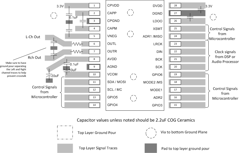
It is recommended to place a top layer ground pour for shielding around the DAC and connect to lower main PCB ground plane by multiple vias
Figure 87. PCM514x Layout Example