ZHCS275D July   2010  – January 2023 TCA6424A

PRODUCTION DATA  

  1. 特性
  2. 说明
  3. Revision History
  4. Description (continued)
  5. Pin Configuration and Functions
  6. Specifications
    1. 6.1 Absolute Maximum Ratings (1)
    2. 6.2 ESD Ratings
    3. 6.3 Recommended Operating Conditions
    4. 6.4 Thermal Information
    5. 6.5 Electrical Characteristics
    6. 6.6 I2C Interface Timing Requirements
    7. 6.7 Reset Timing Requirements
    8. 6.8 Switching Characteristics
    9. 6.9 Typical Characteristics
  7. Parameter Measurement Information
  8. Detailed Description
    1. 8.1 Overview
      1. 8.1.1 Voltage Translation
    2. 8.2 Functional Block Diagram
    3. 8.3 Feature Description
      1. 8.3.1 I/O Port
      2. 8.3.2 I2C Interface
    4. 8.4 Device Functional Modes
      1. 8.4.1 Device Address
    5. 8.5 Programming
      1. 8.5.1 Power-On Reset
      2. 8.5.2 Reset Input ( RESET)
      3. 8.5.3 Interrupt Output ( INT)
      4. 8.5.4 Bus Transactions
        1. 8.5.4.1 Writes
        2. 8.5.4.2 Reads
    6. 8.6 Register Maps
      1. 8.6.1 Control Register and Command Byte
      2. 8.6.2 Register Descriptions
  9. Application and Implementation
    1. 9.1 Typical Application
      1. 9.1.1 Detailed Design Procedure
        1. 9.1.1.1 Minimizing ICC When I/Os Control LEDs
    2. 9.2 Power Supply Recommendation
  10. 10Device and Documentation Support
    1. 10.1 Receiving Notification of Documentation Updates
    2. 10.2 支持资源
    3. 10.3 商标
    4. 10.4 静电放电警告
    5. 10.5 术语表
      1.      Mechanical, Packaging, and Orderable Information

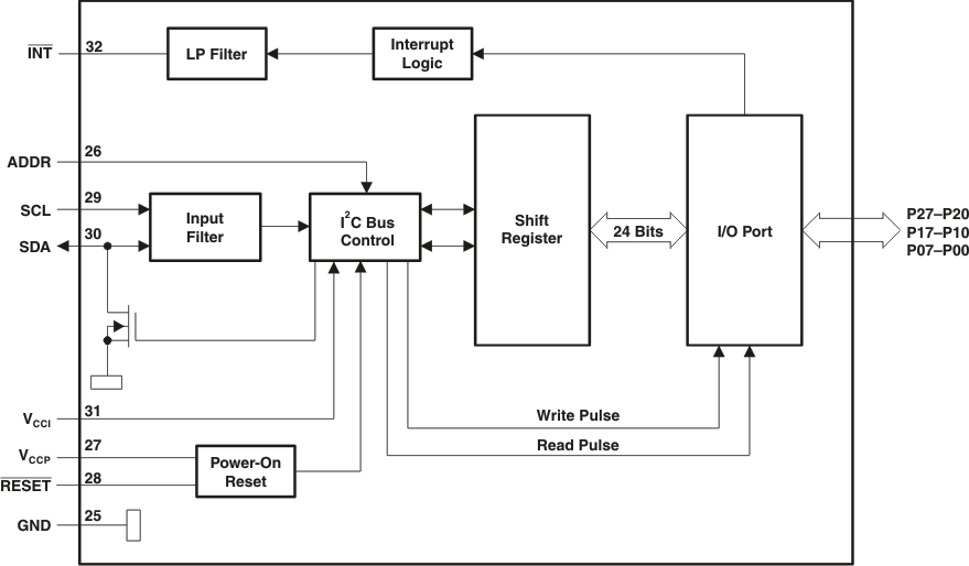
Functional Block Diagram

GUID-0EB21AC6-C5A6-4B37-861E-D7176EDD9081-low.gif
All I/Os are set to inputs at reset.
Pin numbers shown are for the RGJ package.
Figure 8-1 Positive Logic
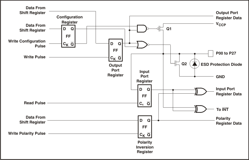
GUID-D27E779F-51DF-4C7D-97D6-41DEEDC190AF-low.gif
On power up or reset, all registers return to default values.
Figure 8-2 Simplified Schematic of P00 to P27