ZHCS310G JANUARY 2009 – September 2015 UCC28610
PRODUCTION DATA.
- 1 特性
- 2 应用
- 3 说明
- 4 修订历史记录
- 5 Pin Configuration and Functions
- 6 Specifications
- 7 Detailed Description
- 8 Application and Implementation
- 9 Power Supply Recommendations
- 10Layout
- 11器件和文档支持
- 12机械、封装和可订购信息
8 Application and Implementation
NOTE
Information in the following applications sections is not part of the TI component specification, and TI does not warrant its accuracy or completeness. TI’s customers are responsible for determining suitability of components for their purposes. Customers should validate and test their design implementation to confirm system functionality.
8.1 Application Information
8.1.1 Transformer Selection
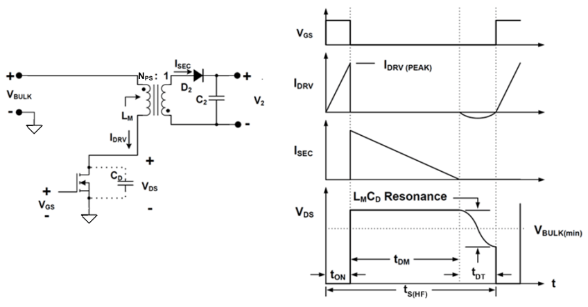
To begin a power supply design, the power supply designer needs to know the peak power to be delivered by the converter, the input voltage range, the output voltage, and an estimate of the maximum allowable bulk voltage ripple. Select the maximum allowable stress voltage for the external power MOSFET. The stress voltage, VDS, determines the reflected secondary voltage that resets the flyback transformer and the turn ratio between primary and secondary. A simplified diagram of the converter and its waveforms are shown in Figure 22.
Peak power is the maximum power level that must be regulated by the converter control system. Loads that last longer than the control loop time constant (100 μs - 300 μs) are directly considered “peak power”. Loads lasting less than the control loop time constant can be averaged over the control loop time constant.
The minimum switching period is when the converter is operating in the Frequency Modulation (FM) mode, referred to as tS(HF). This switching period must equal the sum of the switching intervals at minimum input voltage, maximum load, as shown in Figure 22 and described in Equation 6. The switching intervals are tON, the conduction time of the MOSFET; tDM the demagnetization time of the transformer and tDT, the duration of the deadtime, equal to half of the resonant cycle, after the transformer is de-energized.

Solve for the primary to secondary turn ratio, NPS, using the maximum allowable VDS, the maximum input line voltage, the predicted voltage spike due to leakage inductance and the desired regulated output voltage of the converter, VOUT.
Assume a deadtime, tDT, of 5% of the total minimum switching period to allow for variations in the output capacitance of the HVMOSFET and the leakage inductance value:

Using volt-seconds balance, set the volt-seconds on equal to the volt-seconds for demagnetizing and solve for the on-time:


The maximum input power, PIN, to the converter, in addition to being equal to the output power divided by the overall efficiency, is always equal to:

Solve for the primary inductance value:

This equation is an approximation of the primary inductance value that is the best choice to minimize the primary side RMS current. In the actual circuit, when the resonance and delay due to leakage inductance can be measured, the magnetizing inductance value may need to be iterated for optimized low voltage switching.
Select the CL resistor, RCL, based upon the maximum power constant of the controller, KP, The tolerance of LM should be considered (such as 10% lower for a typical inductor) and the minimum value of LM should be used to calculate the value of the CL resistor.
To avoid tripping the overload protection feature of the controller during the normal operating range, use the minimum value of KP from the Electrical Characteristics Table:

Once RCL is selected, the peak DRV current is calculated using Equation 10:

For high efficiency, the bias winding turn ratio, NPB, should be designed to maintain the VDD voltage above the VGG clamp, which is equal to VGG(DISABLED), when the converter is in burst mode. If VDD discharges below this value, minus the threshold voltage of the HVMOSFET, the HVMOSFET will turn on and linearly supply the VDD current from the high voltage rail instead of from the bias windings. Adding a zener diode on VDD will protect VDD from exceeding its absolute maximum rating in the event of a spike due to excess leakage inductance.
8.1.2 Cascode Bias and Start-Up
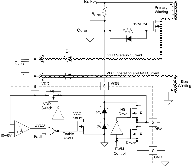
The UCC28610 uses a cascode drive and bias to control the high voltage power MOSFET and provide initial bias at start-up. Thus, the external high voltage power MOSFET provides the start-up function in addition to the power switching function during converter operation. The cascode architecture utilizes a low voltage switch operating between ground and the source of a high voltage MOSFET (HVMOSFET) configured in a common gate configuration, as shown in Figure 23. There are some key points to note.
- The gate of the external HVMOSFET is held at a DC voltage.
- The HVMOSFET is driven through the source, not the gate.
- The entire primary winding current passes through the internal low voltage Driver MOSFET (both DRV and GND pins).
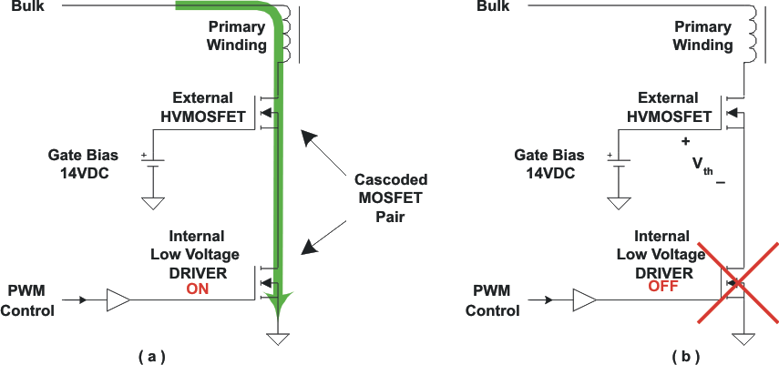 Figure 23. Cascoded Architecture
The UCC28610 integrates the low voltage switch in the form of a 90-mΩ FET along with all associated current sensing and drive. The HVMOSFET is forced to track the fast internal low voltage driver. The drain-gate charge in the HVMOSFET does not affect the turn-off speed because the gate is connected to a low impedance DC source. The cascode configuration results in very fast turn-off of the HVMOSFET, which keeps MOSFET switching losses low.
Cascode drive circuits are well known for high speed voltage gain. This topology can have small signal bandwidth over 100 MHz and it can exhibit high frequency ringing. High frequency ringing can cause EMI problems and become destructive in some situations. The sub-intervals during and immediately following the turn-on and turn-off transients are particularly susceptible to oscillation. For avoidance or solutions, see the application section, Solving High Frequency Ringing.
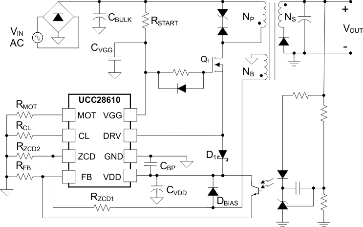
The cascode configuration permits a unique start-up sequence that is fast yet low-loss. Start-up bias uses a low level bleed current from either the AC line or the rectified and filtered AC line, or bulk voltage (via RSTART) as shown in Figure 24. This current charges a small VGG capacitor, CVGG, raising the HVMOSFET gate. The VGG pin will typically draw approximately 6 μA (IVGG(SREG)) during this time, allowing the bulk bias current to be small and still charge the VGG capacitor. The HVMOSFET acts as a source follower once VGG reaches the threshold voltage of the HVMOSFET. Then, the HVMOSFET will bring up the DRV voltage as VGG continues to rise. During this time the UCC28610 is in UVLO and the Enable PWM signal is low. This turns on the VDD switch connecting VDD to DRV, allowing VDD to rise with the source of the HVMOSFET and charging CVDD. An external Schottky diode, D1, is required between DRV and VDD. This diode passes potentially high switching currents that could otherwise flow through the body diode of the internal VDD Switch.
In order to achieve the lowest possible no-load power, select the number of turns in the bias winding so that VDD is higher than 16 V – VTH of the HVMOSFET. A bias winding voltage between 17 V and 20 V usually achieves minimum loss. The bias winding often tracks the primary leakage inductance turn-off voltage spike. Place a 20-V Zener diode between VDD and GND in applications where heavy loads cause excessive VDD voltage.
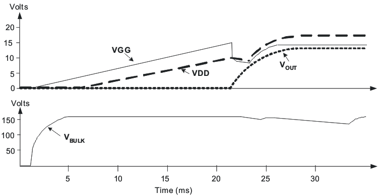 Figure 25. Typical Start-Up Waveforms for a 17-V Bias Winding Voltage
Typical start-up waveforms are shown in Figure 25. As VGG rises, VDD will follow, minus the threshold voltage of the HVMOSFET. When VDD reaches approximately 10 V, the UCC28610 initiates switching. The bias supply current, IVDD, rises to its operating level and it is supplied from the VDD capacitor. Start-up times can be kept under 200 ms by selecting the VGG capacitor in the range of 33 nF to 1000 nF and selecting RSTART to have a current of 15 μA at the minimum AC line voltage. Select capacitor CVDD to have enough capacitance to provide operating bias current to the controller for the time it takes the auxiliary winding to take over. No-load burst operation may impose a requirement for additional CVDD capacitance.
The voltage on VGG is shunt regulated to 16 V whenever the PWM action is disabled. This is reduced to 14 V during switching to limit voltage stress on the gate of the external HVMOSFET. The external HVMOSFET should have a threshold voltage of less than 6 V in order to permit proper starting.
8.1.3 Feedback Function
Modulation and modes are controlled by applying current to the FB pin. The FB pin is usually used to feed back the output error signal to the modulator. The UCC28610 uses internal current mirrors to apply the FB current to the Feedback Processing block, and then to the Frequency Modulator and Current Modulator blocks. The voltage of the FB pin is a constant 0.7 V. AC filtering of the output of the opto-coupler must be applied at the FB pin, as shown in Figure 26. The corner frequency of the filter in Figure 26 should be at least a decade above the maximum switching frequency of the converter, as given in Equation 16. A 100-kΩ resistor, RFB, between the opto-coupler emitter and GND prevents ground noise from resetting the overload timer by biasing the FB pin with a negative current. An opto-coupler with a low Current Transfer Ratio (CTR) is required to give better no-load performance than a high CTR device due to the bias current of the secondary reference. The low CTR also offers better noise immunity than a high CTR device.

8.1.4 Modulation Modes
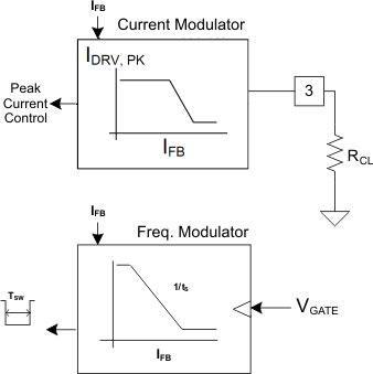
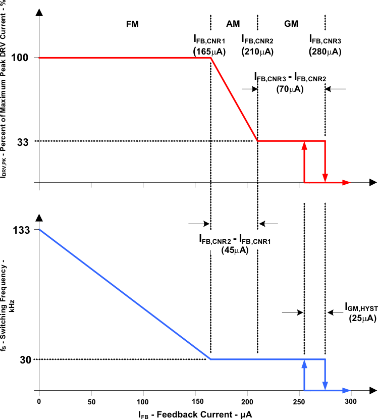
Under normal operating conditions, the FB current commands the operating mode of the UCC28610, as shown in Figure 27 and Figure 28. The FB current commands the UCC28610 to operate the converter in one of three modes: Frequency Modulation (FM) mode, Amplitude Modulation (AM) mode, and Green Mode (GM).
The converter operates in FM mode with a large power load (22% to 100% the peak regulated power). The peak HVMOSFET current reaches its maximum programmed value and FB current regulates the output voltage by varying the switching frequency, which is inversely proportional to tS. The switching frequency is modulated from 30 kHz (22% peak power) to 133 kHz (100% peak power), the on time is constant, and the IDRV peak current is constant. The maximum programmable HVMOSFET current, IDRV,PK(max), is set by a resistor on the CL pin, as described in Equation 15.
The converter operates in AM mode at moderate power levels (2.5% to 22% of the peak regulated power). The FB current regulates the output voltage by modulating the amplitude of the peak HVMOSFET current from 33% to 100% of the maximum programmed value while the switching frequency is fixed at approximately 30 kHz. The UCC28610 modulates the voltage on the CL pin from 3 V to 1 V to vary the commanded peak current, as shown in Figure 27 and Figure 28.
The converter operates in GM at light load (0% to 2.5% of the peak regulated power). The FB current regulates the output voltage in the Green Mode with hysteretic bursts of pulses using FB current thresholds. The peak HVMOSFET current is 33% of the maximum programmed value. The switching frequency within a burst of pulses is approximately 30 kHz. The duration between bursts is regulated by the power supply control dynamics and the FB hysteresis. The UCC28610 reduces internal bias power between bursts in order to conserve energy during light-load and no-load conditions.
8.1.5 Primary Current Sense
The UCC28610 uses a current mirror technique to sense primary current in the Current Modulator. See Figure 29 for details. All of the primary current passes into the DRV pin, through the Driver MOSFET and out of the GND pin. The Driver MOSFET current is scaled and reflected to the PWM Comparator where it is compared with the CL current. At the beginning of each switching cycle a blanking pulse, tBLANK,(Ilim), of approximately 220 ns is applied to the internal current limiter to allow the driver to turn on without false limiting on the leading edge capacitive discharge currents normally present in the circuit.
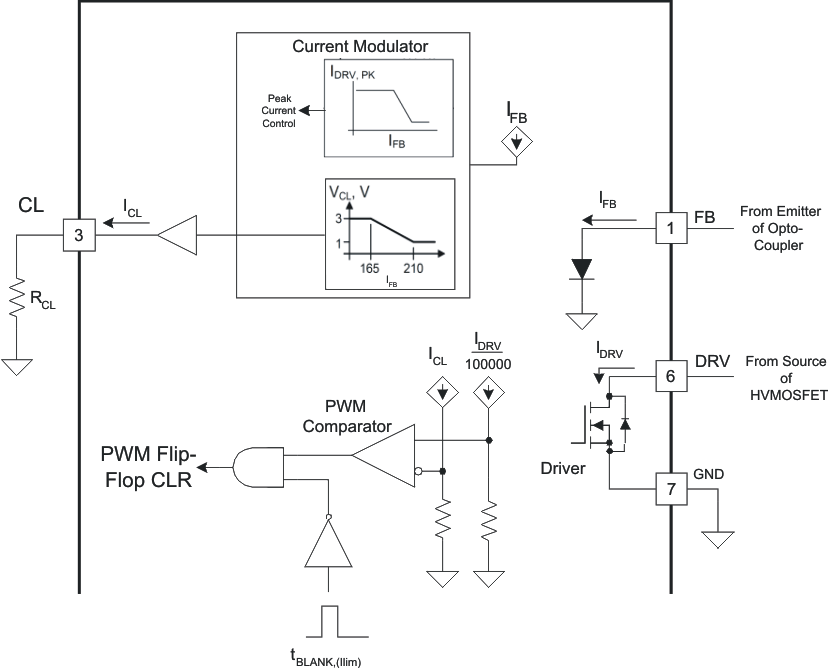 Figure 29. CL pin and DRV Current Sense
8.1.6 Zero Crossing Detection
The modulator requires three conditions in order to initiate the next switching cycle:
- The time since the last turn-on edge must be equal to or greater than the time that is requested by the Feedback Processor as determined by the feedback current, IFB.
- The time since the last turn-on edge must be longer than the minimum period that is built into the UCC28610 (nominally 7.5 μs which equals 133 kHz).
- Immediately following a high-to-low zero crossing of the ZCD voltage. Or, it has been longer than tWAIT,ZCD (~2.4 μs) since the last zero crossing has been detected.
Every switching cycle is preceded by at least one zero crossing detection by the ZCD pin. The modulator allows the resonant ring to damp between pulses if the period needs to exceed the damping limit, allowing long pauses between pulses during no-load operation.
The switching frequency is not allowed to exceed 133 kHz (nominally). This sets the maximum power limit so that it will be constant for all bulk voltages that exceed the minimum line voltage value.
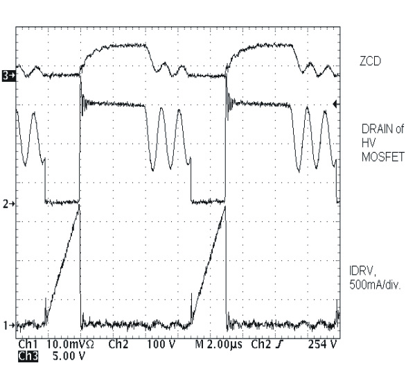
Figure 30 illustrates a set of switching cycle waveforms over a range of operating conditions. The UCC28610 is designed to always keep the inductor current discontinuous. This prevents current tailing during start-up or short circuit conditions and accommodates control of the maximum power delivered.
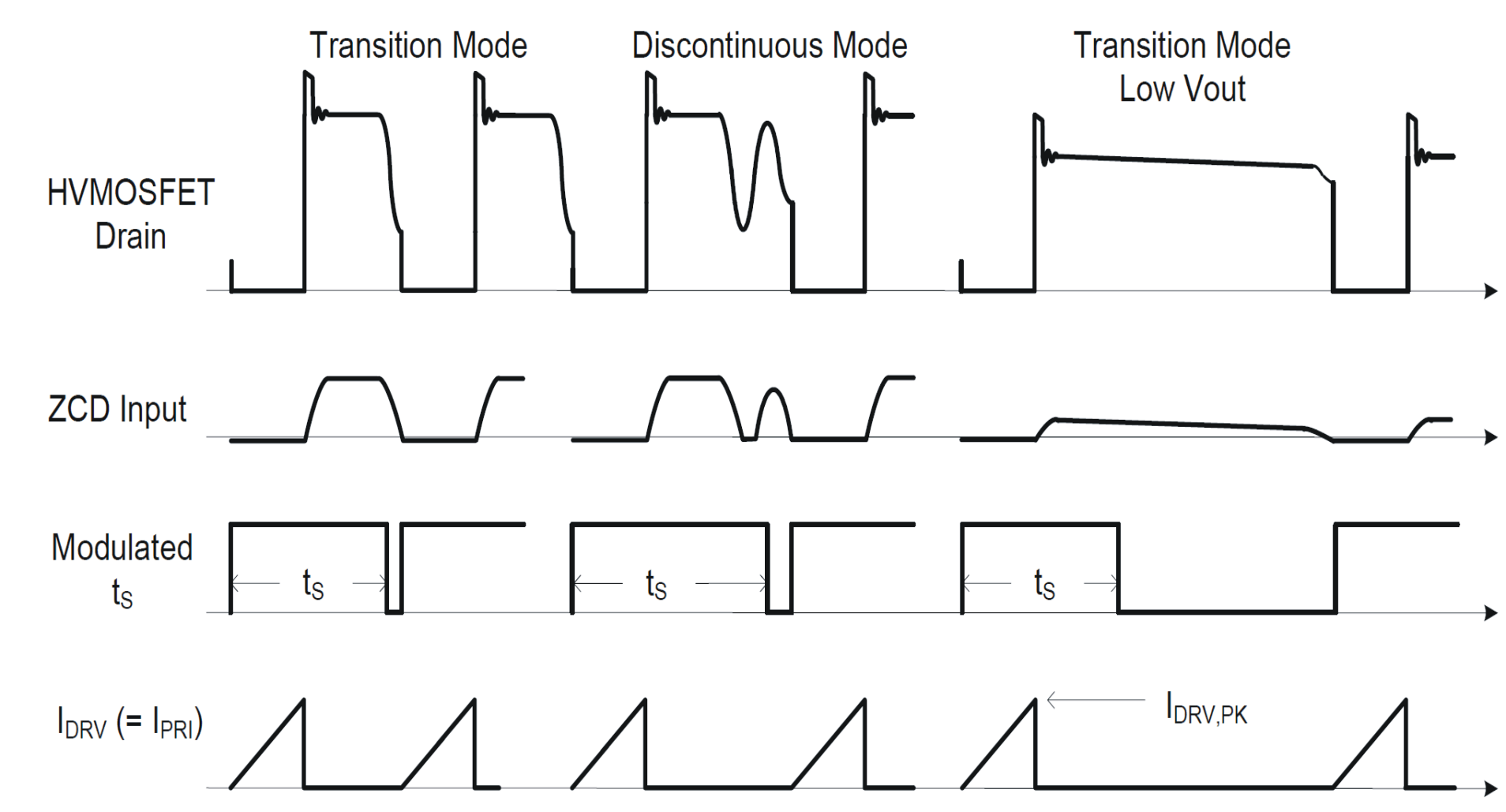 Figure 30. Switching Cycle Waveforms
Zero crossing is detected using a resistive divider across the bias winding, as shown in Figure 31. The bias winding operates in phase with the output winding. The ZCD function detects transformer demagnetization when the ZCD voltage has a high to low crossing of the 20-mV ZCD threshold, ZCDTH. The voltage at the ZCD pin is internally clamped to contain negative excursions at -160mV (ZCDCLAMP). A small delay, 50 ns to 200 ns, can be added with CZCD to align the turn-on of the primary switch with the resonant valley of the primary winding waveform.
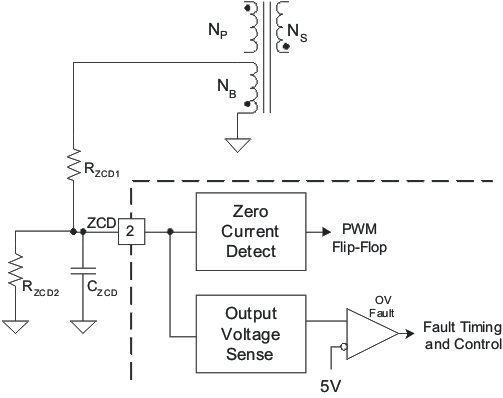 Figure 31. Zero Crossing Detection


8.1.7 Green Mode Operation
During light load operation the UCC28610 cycles between two states: GM-on and GM-off. The details are shown in Figure 32. During the GM-on state, the controller is active while the modulator issues a burst of one or more pulses. During the GM-off state the controller reduces its operating current and switching action is inhibited. The rate and duration of the on and off states are controlled by the current into the FB pin as it cycles between the two hysteretic thresholds separated by IFB, GM_HYST, the load current, the output filter capacitor, and the details of the feedback circuit.
During the GM-off state the VDD supply current is reduced to approximately 550 μA, IVDD(GM). The Enable PWM signal goes low which inhibits switching, sets the VGG shunt regulation to ~16 V, VGG(DISABLED), and turns on the VDD switch. The VGG node quickly charges to 16V and the low VDD current is supplied from the VDD capacitor.
During the GM-on state the UCC28610 controls the peak primary current to 33% of IDRV,PK(max), at a 30-kHz rate. When switching, the VGG shunt regulator pulls the VGG voltage down to ~14 V. VDD is charged by the auxiliary winding during this time as long as VDD does not discharge below 14 V. The converter’s output voltage is charged until the feedback network forces the FB current to the GM off threshold, IFB,CNR3, and puts the controller back into the GM off state.
At very light loads the time between PWM bursts can be long. To obtain the lowest no-load power, it is important that VDD not discharge below 16 V by more than the threshold voltage of the HVMOSFET or the HVMOSFET will turn-on and linearly supply the VDD current from the high-voltage bulk rail. The VDD voltage can be extended by increasing the CVDD capacitance without significant impact on start-up time.
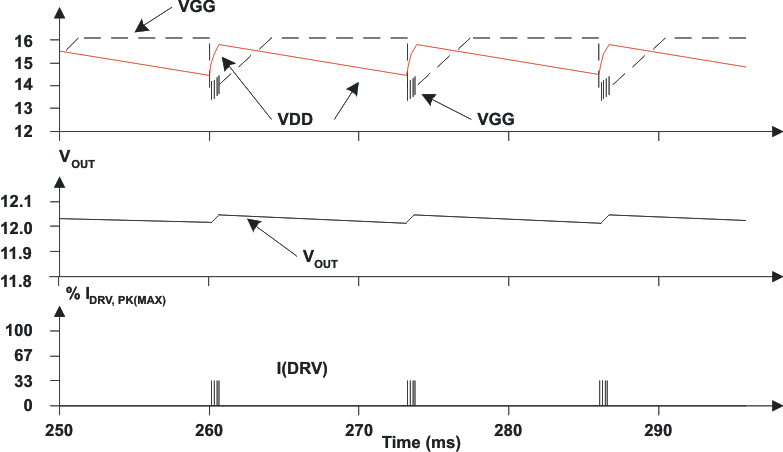 Figure 32. Green Mode Operation
8.1.8 Maximum Converter Power Limitation
The suggested peak power range of the UCC28610 is 12 W to 65 W based on a universal AC line converter (90-VAC to 265-VAC input line voltage), using an external high voltage MOSFET with a voltage rating of 600 V. This power range may depend on application and external MOSFET stress voltage. Ultimately, the peak primary current is the limiting factor because this current must pass through the UCC28610. The limit on the peak primary current imposes a limit on the peak primary power. The peak power must be less than 65 W, not the average power. The peak power is defined as the highest power level where the controller must maintain regulation.
At all power levels, program the UCC28610 to control the power limit with the primary inductance, peak current and maximum switching frequency (133 kHz). The maximum peak input power level is given by Equation 19. The accuracy of the power limit is twice as sensitive to IDRV(PK) errors than LM errors and fS(max) errors. If the load demands more power than the programmed level, the power supply output voltage sags and the overload timer is initiated.

8.1.9 Minimum Converter Power Limitation
The dynamics of the DRV current sense imposes the 12-W minimum power level limit for this controller. The power level limits are found from DRV current estimates for typical universal AC adapters that use a 600-V MOSFET. The power range and its associated peak current range are given in Equation 20.

The minimum power level is due to a loss of linearity of the current mirror, as shown in Figure 33. A programmed IDRV,PK level between 0.66 A and 1 A (by using 100 kΩ ≤ RCL ≤ 150 kΩ) allows only a 2:1 amplitude modulation range of the peak DRV current. The amplitude of IDRV modulates linearly if IDRV,PK is programmed within its recommended operating range (1.0 A < IDRV,PK < 4.1 A, corresponding to 100 kΩ > RCL > 24.3 kΩ respectively.
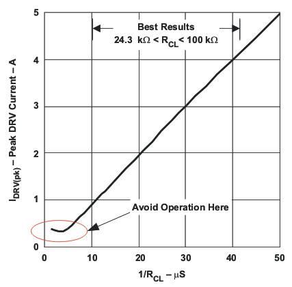 Figure 33. Dynamic Operating Range
8.2 Typical Application
8.2.1 Design Requirements
Table 1 illustrates a typical subset of high-level design requirements. Many of these parameter values are used in the design equations contained in Table 2.
Table 1. UCC28610EVM-474 Electrical Performance Specifications
| PARAMETER | CONDITIONS | MIN | NOM | MAX | UNIT | |
|---|---|---|---|---|---|---|
| INPUT CHARACTERISTICS | ||||||
| VIN | Input voltage | 85 | 265 | VRMS | ||
| OUTPUT CHARACTERISTICS | ||||||
| VOUT | Output voltage | VIN = min to max, IOUT = min to max | 10.8 | 12 | 13.2 | V |
| Vripple | Output voltage ripple | VIN = 115 VRMS, IOUT = max | 80 | 120 | mVpp | |
| IOUT | Output current | VIN = min to max | 0 | 2.1 | A | |
| IOCP | Output over current inception point | VIN = max | 3 | A | ||
| VOVP | Output OVP | IOUT = min to max | 16 | V | ||
| Transient response voltage over shoot | IOUT = min to max | 500 | mV | |||
| SYSTEM CHARACTERISTICS | ||||||
| hPEAK | Peak efficiency | VIN = 115 VRMS, IOUT = 1.05 A | 85.7% | |||
| No load power consumption | VIN = 115 VRMS | 67 | mW | |||
| VIN = 230 VRMS | 107 | |||||
For reference designators refer to Figure 34.
8.2.2 Detailed Design Procedure
Table 2. Pin Components(1)(2)
| NAME | PIN | DESCRIPTION |
|---|---|---|
| CL | 3 |  |
 |
||
| Where KP = 0.54W/ μH | ||
| LM is the minimum value of the primary inductance | ||
| PIN = POUT/η | ||
| η = efficiency | ||
| DRV | 6 | Q1, power MOSFET with adequate voltage and current ratings, VVGS must have at least 20-V static rating. |
| D1, Schottky diode, rated for at least 30 V, placed between DRV and VDD | ||
| FB | 1 | RFB = 100 kΩ |
| GND | 7 | Bypass capacitor to VDD, CBP = 0.1-μF, ceramic |
| MOT | 4 | For latch-off response to overcurrent faults: |
| tMOT = user programmable maximum on-time after 250-ms delay. | ||
 where
|
||
| For shutdown-retry response to overcurrent faults: | ||

|
||
| VDD | 8 |  |
| where: | ||
| ΔVDD(BURST) is the allowed VDD ripple during burst operation | ||
| tBURST is the estimated burst period, | ||
| The typical CVDD value is approximately 47 μF | ||
| DBIAS must have a voltage rating greater than: | ||
 |
||
| where: | ||
| VDBIAS is the reverse voltage rating of diode D2 | ||
| VBULK(max) is the maximum rectified voltage of CBULK at the highest line voltage | ||
| VGG | 5 | minimize the length of the CVGG connection to GND |
| CVGG = at least 10x CGS of HVMOSFET, usually | ||
| CVGG = 0.1 μF. | ||
| ZCD | 2 |   |
| where: | ||
| ZCD(ovp) is the overvoltage fault threshold at ZCD | ||
| NPS is the primary to secondary turns ratio | ||
| NPB is the primary to bias turns ratio | ||
| VOUT is the average output voltage of the secondary | ||
| VF is the forward bias voltage of the secondary rectifier | ||
| VOUT,PEAK is the desired output overvoltage fault level |
8.2.2.1 Input Bulk Capacitance and Minimum Bulk Voltage
Bulk capacitance may consist of one or more capacitors connected in parallel. The input power of the converter based on target full-load efficiency, minimum input RMS voltage, minimum AC input frequency, and minimum bulk capacitor voltage are used to determine the bulk capacitor value. Maximum input power is used in the CBULK calculation and is determined by:

Assume 30% voltage ripple on the bulk capacitor, the minimum bulk capacitor voltage is 70% of the minimum input AC voltage at its peak value.

Equation 23 provides an accurate solution for input capacitance needed to achieve a minimum bulk valley voltage target VBULK(min), accounting for hold-up during any loss of AC power for a certain number of half cycles, NHC, by an AC-line drop-out condition. Alternatively, if a given input capacitance value is prescribed, iterate the VBULK(min) value until that target capacitance is obtained, which determines the VBULK(min) expected for that capacitance.

8.2.2.2 Transformer Selection
To begin a power supply design, the power supply designer needs to know the peak power to be delivered by the converter, the input voltage range, the output voltage, and an estimate of the maximum allowable bulk voltage ripple. Select the maximum allowable stress voltage for the external power MOSFET. The stress voltage, VDS, determines the reflected secondary voltage that resets the flyback transformer and the turn ratio between primary and secondary. A simplified diagram of the converter and its waveforms are shown in Figure 22.
Peak power is the maximum power level that must be regulated by the converter control system. Loads that last longer than the control loop time constant (100 μs - 300 μs) are directly considered “peak power”. Loads lasting less than the control loop time constant can be averaged over the control loop time constant.
The minimum switching period is when the converter is operating in the Frequency Modulation (FM) mode, referred to as tS(HF). This switching period must equal the sum of the switching intervals at minimum input voltage, maximum load, as shown in Figure 35 and described in Equation 24. The switching intervals are tON, the conduction time of the MOSFET; tDM the demagnetization time of the transformer and tDT, the duration of the deadtime, equal to half of the resonant cycle, after the transformer is de-energized.

Solve for the primary to secondary turn ratio, NPS, using the maximum allowable VDS, the maximum input line voltage, the predicted voltage spike due to leakage inductance and the desired regulated output voltage of the converter, VOUT.
Assume a deadtime, tDT, of 5% of the total minimum switching period to allow for variations in the output capacitance of the HVMOSFET and the leakage inductance value:

Using volt-seconds balance, set the volt-seconds on equal to the volt-seconds for demagnetizing and solve for the on-time:


The maximum input power, PIN, to the converter, in addition to being equal to the output power divided by the overall efficiency, is always equal to:

Solve for the primary inductance value:

This equation is an approximation of the primary inductance value that is the best choice to minimize the primary side RMS current. In the actual circuit, when the resonance and delay due to leakage inductance can be measured, the magnetizing inductance value may need to be iterated for optimized low voltage switching.
Select the CL resistor, RCL, based upon the maximum power constant of the controller, KP, The tolerance of LM should be considered (such as 10% lower for a typical inductor) and the minimum value of LM should be used to calculate the value of the CL resistor.
To avoid tripping the overload protection feature of the controller during the normal operating range, use the minimum value of KP from the Electrical Characteristics Table:

Once RCL is selected, the peak DRV current is calculated using Equation 10:

For high efficiency, the bias winding turn ratio, NPB, should be designed to maintain the VDD voltage above the VGG clamp, which is equal to VGG(DISABLED), when the converter is in burst mode. If VDD discharges below this value, minus the threshold voltage of the HVMOSFET, the HVMOSFET will turn on and linearly supply the VDD current from the high voltage rail instead of from the bias windings. Adding a zener diode on VDD will protect VDD from exceeding its absolute maximum rating in the event of a spike due to excess leakage inductance.
8.2.2.3 Feedback Function
Modulation and modes are controlled by applying current to the FB pin. The FB pin is usually used to feed back the output error signal to the modulator. The UCC28610 uses internal current mirrors to apply the FB current to the Feedback Processing block, and then to the Frequency Modulator and Current Modulator blocks. The voltage of the FB pin is a constant 0.7 V. AC filtering of the output of the opto-coupler must be applied at the FB pin, as shown in Figure 36. The corner frequency of the filter in Figure 36 should be at least a decade above the maximum switching frequency of the converter, as given in Equation 34. A 100-kΩ resistor, RFB, between the opto-coupler emitter and GND prevents ground noise from resetting the overload timer by biasing the FB pin with a negative current. An opto-coupler with a low Current Transfer Ratio (CTR) is required to give better no-load performance than a high CTR device due to the bias current of the secondary reference. The low CTR also offers better noise immunity than a high CTR device.

Zero crossing is detected using a resistive divider across the bias winding, as shown in Figure 37. The bias winding operates in phase with the output winding. The ZCD function detects transformer demagnetization when the ZCD voltage has a high to low crossing of the 20-mV ZCD threshold, ZCDTH. The voltage at the ZCD pin is internally clamped to contain negative excursions at -160mV (ZCDCLAMP). A small delay, 50 ns to 200 ns, can be added with CZCD to align the turn-on of the primary switch with the resonant valley of the primary winding waveform.
 Figure 37. Zero Crossing Detection


8.2.3 Application Curves
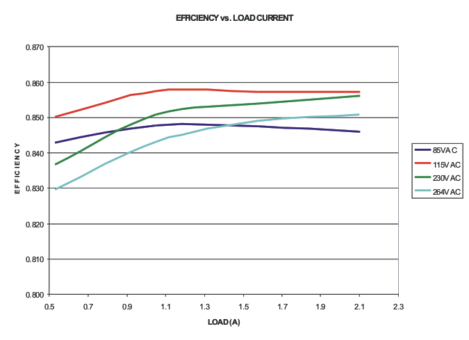 Figure 38. Efficiency as a Function of Load Current and Input Voltage
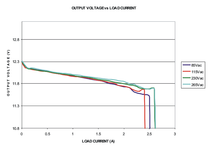
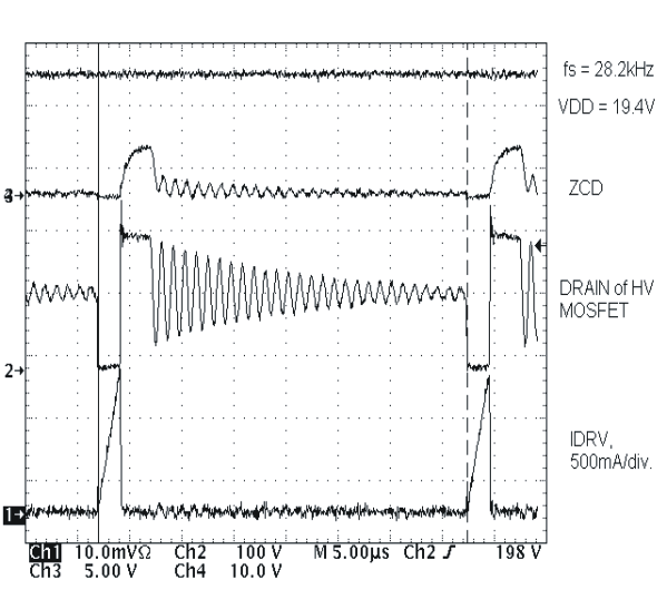
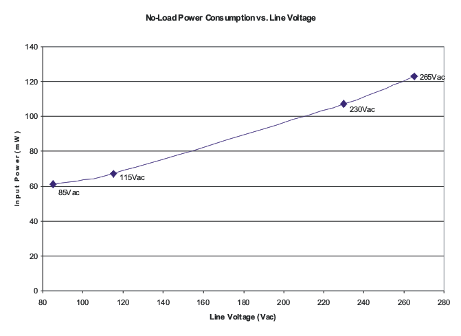 Figure 39. No-Load Input Power as a Function of Input Voltage
