ZHCS311D May   2009  – January 2018 ADS1113 , ADS1114 , ADS1115

PRODUCTION DATA.  

  1. 特性
  2. 应用
  3. 说明
    1.     Device Images
      1.      简化的方框图
  4. Revision History
  5. Device Comparison Table
  6. Pin Configuration and Functions
    1.     Pin Functions
  7. Specifications
    1. 7.1 Absolute Maximum Ratings
    2. 7.2 ESD Ratings
    3. 7.3 Recommended Operating Conditions
    4. 7.4 Thermal Information
    5. 7.5 Electrical Characteristics
    6. 7.6 Timing Requirements: I2C
    7. 7.7 Typical Characteristics
  8. Parameter Measurement Information
    1. 8.1 Noise Performance
  9. Detailed Description
    1. 9.1 Overview
    2. 9.2 Functional Block Diagrams
    3. 9.3 Feature Description
      1. 9.3.1 Multiplexer
      2. 9.3.2 Analog Inputs
      3. 9.3.3 Full-Scale Range (FSR) and LSB Size
      4. 9.3.4 Voltage Reference
      5. 9.3.5 Oscillator
      6. 9.3.6 Output Data Rate and Conversion Time
      7. 9.3.7 Digital Comparator (ADS1114 and ADS1115 Only)
      8. 9.3.8 Conversion Ready Pin (ADS1114 and ADS1115 Only)
      9. 9.3.9 SMbus Alert Response
    4. 9.4 Device Functional Modes
      1. 9.4.1 Reset and Power-Up
      2. 9.4.2 Operating Modes
        1. 9.4.2.1 Single-Shot Mode
        2. 9.4.2.2 Continuous-Conversion Mode
      3. 9.4.3 Duty Cycling For Low Power
    5. 9.5 Programming
      1. 9.5.1 I2C Interface
        1. 9.5.1.1 I2C Address Selection
        2. 9.5.1.2 I2C General Call
        3. 9.5.1.3 I2C Speed Modes
      2. 9.5.2 Slave Mode Operations
        1. 9.5.2.1 Receive Mode
        2. 9.5.2.2 Transmit Mode
      3. 9.5.3 Writing To and Reading From the Registers
      4. 9.5.4 Data Format
    6. 9.6 Register Map
      1. 9.6.1 Address Pointer Register (address = N/A) [reset = N/A]
        1. Table 6. Address Pointer Register Field Descriptions
      2. 9.6.2 Conversion Register (P[1:0] = 0h) [reset = 0000h]
        1. Table 7. Conversion Register Field Descriptions
      3. 9.6.3 Config Register (P[1:0] = 1h) [reset = 8583h]
        1. Table 8. Config Register Field Descriptions
      4. 9.6.4 Lo_thresh (P[1:0] = 2h) [reset = 8000h] and Hi_thresh (P[1:0] = 3h) [reset = 7FFFh] Registers
        1. Table 9. Lo_thresh and Hi_thresh Register Field Descriptions
  10. 10Application and Implementation
    1. 10.1 Application Information
      1. 10.1.1 Basic Connections
      2. 10.1.2 Single-Ended Inputs
      3. 10.1.3 Input Protection
      4. 10.1.4 Unused Inputs and Outputs
      5. 10.1.5 Analog Input Filtering
      6. 10.1.6 Connecting Multiple Devices
      7. 10.1.7 Quickstart Guide
    2. 10.2 Typical Application
      1. 10.2.1 Design Requirements
      2. 10.2.2 Detailed Design Procedure
        1. 10.2.2.1 Shunt Resistor Considerations
        2. 10.2.2.2 Operational Amplifier Considerations
        3. 10.2.2.3 ADC Input Common-Mode Considerations
        4. 10.2.2.4 Resistor (R1, R2, R3, R4) Considerations
        5. 10.2.2.5 Noise and Input Impedance Considerations
        6. 10.2.2.6 First-order RC Filter Considerations
        7. 10.2.2.7 Circuit Implementation
        8. 10.2.2.8 Results Summary
      3. 10.2.3 Application Curves
  11. 11Power Supply Recommendations
    1. 11.1 Power-Supply Sequencing
    2. 11.2 Power-Supply Decoupling
  12. 12Layout
    1. 12.1 Layout Guidelines
    2. 12.2 Layout Example
  13. 13器件和文档支持
    1. 13.1 Documentation Support
      1. 13.1.1 相关文档
    2. 13.2 相关链接
    3. 13.3 Receiving Notification of Documentation Updates
    4. 13.4 社区资源
    5. 13.5 商标
    6. 13.6 静电放电警告
    7. 13.7 Glossary
  14. 14机械、封装和可订购信息

Basic Connections

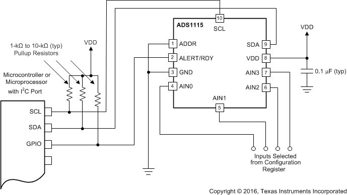
The principle I2C connections for the ADS1115 are shown in Figure 39.

ADS1113 ADS1114 ADS1115 ai_typ_connex_bas444.gifFigure 39. Typical Connections of the ADS1115

The fully-differential voltage input of the ADS111x is ideal for connection to differential sources with moderately low source impedance, such as thermocouples and thermistors. Although the ADS111x can read bipolar differential signals, these devices cannot accept negative voltages on either input.

The ADS111x draw transient currents during conversion. A 0.1-μF power-supply bypass capacitor supplies the momentary bursts of extra current required from the supply.

The ADS111x interface directly to standard mode, fast mode, and high-speed mode I2C controllers. Any microcontroller I2C peripheral, including master-only and single-master I2C peripherals, operates with the ADS111x. The ADS111x does not perform clock-stretching (that is, the device never pulls the clock line low), so it is not necessary to provide for this function unless other clock-stretching devices are on the same I2C bus.

Pullup resistors are required on both the SDA and SCL lines because I2C bus drivers are open drain. The size of these resistors depends on the bus operating speed and capacitance of the bus lines. Higher-value resistors consume less power, but increase the transition times on the bus, thus limiting the bus speed. Lower-value resistors allow higher speed, but at the expense of higher power consumption. Long bus lines have higher capacitance and require smaller pullup resistors to compensate. Do not use resistors that are too small because the bus drivers may not be able to pull the bus lines low.