ZHCS327D July 2011 – October 2016 BQ76925
PRODUCTION DATA.
- 1 特性
- 2 应用
- 3 说明
- 4 修订历史记录
- 5 说明 (续)
- 6 Pin Configuration and Functions
-
7 Specifications
- 7.1 Absolute Maximum Ratings
- 7.2 ESD Ratings
- 7.3 Recommended Operating Conditions
- 7.4 Thermal Information
- 7.5 Electrical Characteristics: Supply Current
- 7.6 Internal Power Control (Startup and Shutdown)
- 7.7 3.3-V Voltage Regulator
- 7.8 Voltage Reference
- 7.9 Cell Voltage Amplifier
- 7.10 Current Sense Amplifier
- 7.11 Overcurrent Comparator
- 7.12 Internal Temperature Measurement
- 7.13 Cell Balancing and Open Cell Detection
- 7.14 I2C Compatible Interface
- 7.15 Typical Characteristics
-
8 Detailed Description
- 8.1 Overview
- 8.2 Functional Block Diagram
- 8.3 Feature Description
- 8.4 Device Functional Modes
- 8.5 Programming
- 8.6 Register Maps
- 9 Application and Implementation
- 10Power Supply Recommendations
- 11Layout
- 12器件和文档支持
- 13机械、封装和可订购信息
9 Application and Implementation
NOTE
Information in the following applications sections is not part of the TI component specification, and TI does not warrant its accuracy or completeness. TI’s customers are responsible for determining suitability of components for their purposes. Customers should validate and test their design implementation to confirm system functionality.
9.1 Application Information
The bq76925 device is a host-controlled analog front end (AFE), providing the individual cell voltages, pack current, and temperature to the host system. The host controller may use this information to complete the pack monitoring, balancing, and protection functions for the 3-series to 6-series cell Li-ion/Li-Polymer battery.
The section below highlights several recommended implementations when using this device. A detailed bq76925 Application report, SLUA619, together with an example implementation report using bq76925 and MSP430G2xx2, SLUA707, are available at www.ti.com.
9.1.1 Recommended System Implementation
9.1.1.1 Voltage, Current, and Temperature Outputs
The bq76925 device provides voltage, current, and temperature outputs in analog form. A microcontroller (MCU) with an analog-to-digital converter (ADC) is required to complete the measurement system. A minimum of three input-ADC channels of the MCU are required to measure cell voltages, current, and temperature output. The bq76925 device can supply an external reference for the MCU ADC reference, Compare the internal reference voltage specification of the MCU to determine if using the AFE reference would improve the measurement accuracy.
9.1.1.2 Power Management
The bq76925 device can disable varies functions for power management. Refer to the POWER_CTL registers in this document for detailed descriptions. Additionally, the MCU can put the bq76925 device into SHUTDOWN mode by writing to the [SLEEP] bit in the POWER_CTL register. The wake up circuit does not activate until the V3P3 is completing discharge to 0 V. Once the wake up circuit is activated, pulling the ALERT pin high can wake up the device. This means, once the SLEEP command is sent, the bq76925 device remains in SHUTDOWN mode and cannot wake up if V3P3 is > 0 V.
9.1.1.3 Low Dropout (LDO) Regulator
When the LDO load current is higher than 4 mA, the LDO must be used with an external pass transistor. In this configuration, a high-gain bypass device is recommended. ZXTP2504DFH and IRLML9303 are example transistors. A Z1 diode is recommended to protect the gate-source or base emitter of the bypass transistor.
Adding the RV3P3 and CV3P3-2 filter helps to isolate the load from the V3P3 transient caused by the load and the transients on BAT.
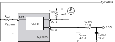 Figure 15. LDO Regulator
9.1.1.4 Input Filters
TI recommends to use input filters for BAT, VCx, and SENSEN/P pins to protect the bq76925 device from large transients caused by switching of the battery load.
Additionally, the filter on BAT also avoids unintentional reset of the AFE when the battery voltage suddenly drops. To further avoid an unwanted reset, a hold-up circuit using a blocking diode can be added in series with the input filter. A zener diode clamp may be added in parallel with the filter capacitor to prevent the repeated peak transients that pump up the filter capacitor beyond the device absolute maximum rating.
9.1.1.5 Output Filters
Output capacitors are used on V3P3, VREF, VCOUT, and VIOUT for stability. These capacitors also function as bypass capacitors in response to the MCU internal switching and ADC operation. Additional filtering may be added to these output pins to smooth out noisy signals prior to ADC conversion. For the V3P3 case, an additional filter helps reduce the transient on the power input connected to the bq76925 device's V3P3 pin.
9.1.2 Cell Balancing
The bq76925 device integrates cell balancing FETs that are controlled individually by the host. The device does not automatically duty cycle the balancing FETs such that cell voltage measurement for protection detection is taken when balancing is off. The host MCU is responsible for such management. Otherwise, the MCU is free to turn on the voltage measurement during cell balancing, which enables the open-cell detection method described in this document. However, the bq76925 device does prevent two adjacent balancing FETs from being turned on simultaneously. If such a condition occurs, both adjacent transistors will remain off.
9.2 Typical Application
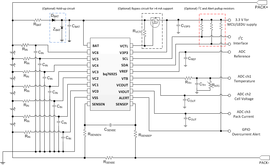 Figure 16. Typical Schematic
9.2.1 Design Requirements
For this design example, use the parameters listed in Table 27.
Table 27. Design Parameters
| PARAMETER | MIN | TYP | MAX | UNIT | |||
|---|---|---|---|---|---|---|---|
| RBAT | BAT filter resistance | 100 | Ω | ||||
| CBAT | BAT filter capacitance | 10 | µF | ||||
| RIN | External cell input resistance | (1) | 100 | Ω | |||
| CIN | External cell input capacitance | 0.1 | 1 | 10 | µF | ||
| RSENSEN
RSENSEP |
Current sense input filter resistance | 1K | Ω | ||||
| CSENSE | Current sense input filter capacitance | 0.1 | µF | ||||
| RVCTL | VCTL pullup resistance | Without external bypass transistor | 0 | Ω | |||
| With external bypass transistor | 200K | ||||||
| CV3P3 | V3P3 output capacitance | Without external bypass transistor | 4.7 | µF | |||
| With external bypass transistor | 1.0 | ||||||
| CREF | VREF output capacitance | 1.0 | µF | ||||
| COUT | ADC channel output capacitance | VCOUT | 0.1 | µF | |||
| VIOUT | 470 | 2000 | pF | ||||
9.2.2 Detailed Design Procedure
The following is the detailed design procedure.
- Select a proper MCU to complete the battery management solution. Refer to the bq76925 Application report, SLUA619 on MCU requirement.
- Based on the system design, determine if an alternative cell connection for 4-series and 5- series battery pack is needed. Refer to the “Cell Amplifier Headroom Under BAT Voltage Drop” section of this document.
- Determine if a hold-up circuit for BAT and/or an external bypass transistor is needed based on the system design. Follow the reference schematic to complete the circuit design.
- An example circuit design and MCU code implementation is documented in SLUA707 using bq79625 and MSP430G2xx2.
9.2.3 Application Curves
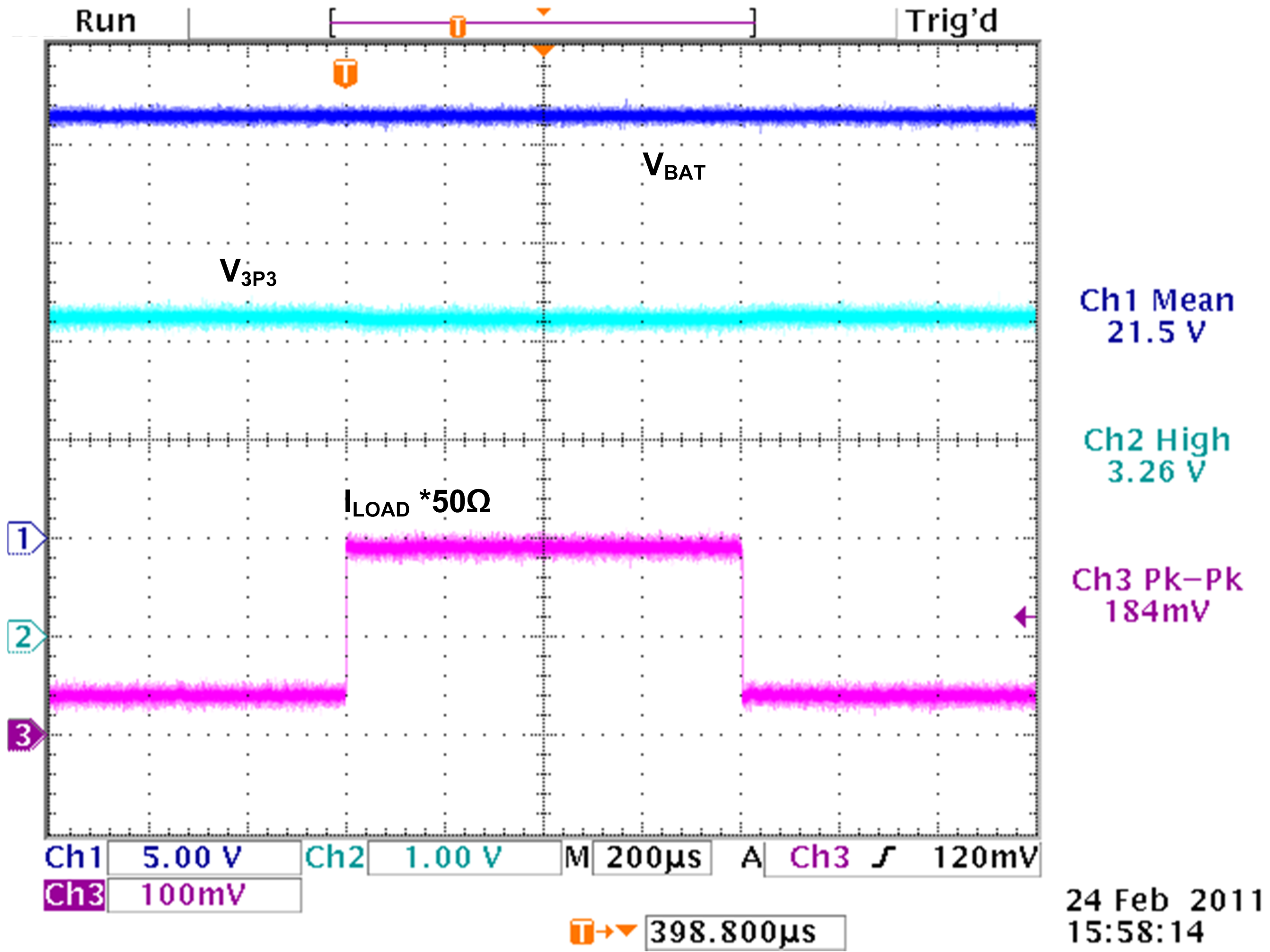
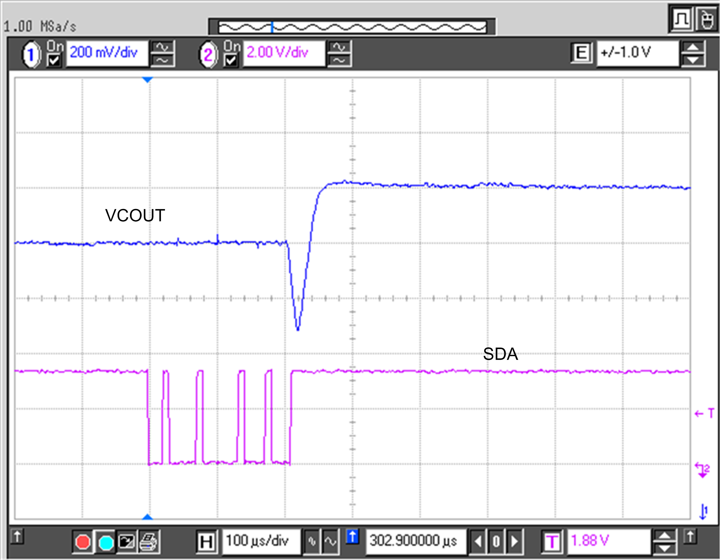
| Load step = 3.7 mA | ||
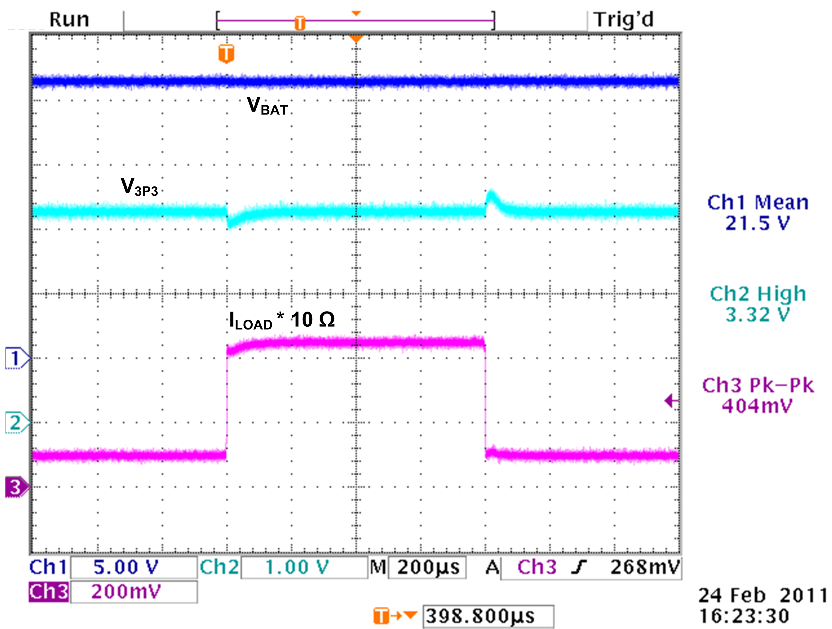
| Load step = 40.4 mA | ||
