ZHCS327D July 2011 – October 2016 BQ76925
PRODUCTION DATA.
- 1 特性
- 2 应用
- 3 说明
- 4 修订历史记录
- 5 说明 (续)
- 6 Pin Configuration and Functions
-
7 Specifications
- 7.1 Absolute Maximum Ratings
- 7.2 ESD Ratings
- 7.3 Recommended Operating Conditions
- 7.4 Thermal Information
- 7.5 Electrical Characteristics: Supply Current
- 7.6 Internal Power Control (Startup and Shutdown)
- 7.7 3.3-V Voltage Regulator
- 7.8 Voltage Reference
- 7.9 Cell Voltage Amplifier
- 7.10 Current Sense Amplifier
- 7.11 Overcurrent Comparator
- 7.12 Internal Temperature Measurement
- 7.13 Cell Balancing and Open Cell Detection
- 7.14 I2C Compatible Interface
- 7.15 Typical Characteristics
-
8 Detailed Description
- 8.1 Overview
- 8.2 Functional Block Diagram
- 8.3 Feature Description
- 8.4 Device Functional Modes
- 8.5 Programming
- 8.6 Register Maps
- 9 Application and Implementation
- 10Power Supply Recommendations
- 11Layout
- 12器件和文档支持
- 13机械、封装和可订购信息
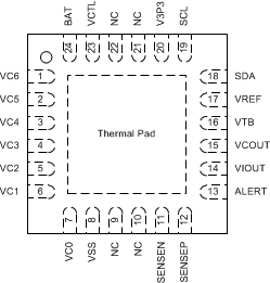
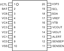
6 Pin Configuration and Functions
RGE Package
24-Pin QFN With Thermal Pad
Top View

Pin Functions
| NAME | PIN NO. | TYPE | DESCRIPTION | |
|---|---|---|---|---|
| TSSOP | VQFN | |||
| VCTL | 1 | 23 | Output | 3.3-V Regulator control voltage(1) |
| ALERT | 13 | 13 | Output | Overcurrent alert (open drain) |
| BAT | 2 | 24 | Power | Supply voltage, tied to most positive cell |
| NC | — | 9, 10, 21, 22 | — | No Connection (leave open) |
| SCL | 19 | 19 | Input | I2C Clock (open drain) |
| SDA | 18 | 18 | Input / Output | I2C Data (open drain) |
| SENSEN | 11 | 11 | Input | Negative current sense |
| SENSEP | 12 | 12 | Input | Positive current sense |
| V3P3 | 20 | 20 | Output | 3.3-V Regulator |
| VC6 | 3 | 1 | Input | Sense voltage for most positive cell |
| VC5 | 4 | 2 | Input | Sense voltage for second most positive cell |
| VC4 | 5 | 3 | Input | Sense voltage for third most positive cell |
| VC3 | 6 | 4 | Input | Sense voltage for fourth most positive cell |
| VC2 | 7 | 5 | Input | Sense voltage for fifth most positive cell |
| VC1 | 8 | 6 | Input | Sense voltage for least positive cell |
| VC0 | 9 | 7 | Input | Sense voltage for negative end of cell stack |
| VCOUT | 15 | 15 | Output | Cell measurement voltage |
| VIOUT | 14 | 14 | Output | Current measurement voltage |
| VREF | 17 | 17 | Output | Reference voltage for ADC |
| VSS | 10 | 8 | Power | Ground |
| VTB | 16 | 16 | Output | Bias voltage for thermistor network |
(1) When a bypass FET is used to supply the regulated 3.3-V load current, VCTL automatically adjusts to keep V3P3 = 3.3 V. If VCTL is tied to BAT, the load current is supplied through V3P3.
