ZHCS363L August 2011 – March 2017 TRF7970A
PRODUCTION DATA.
- 1器件概述
- 2修订历史记录
- 3Device Characteristics
- 4Terminal Configuration and Functions
- 5Specifications
-
6Detailed Description
- 6.1 Overview
- 6.2 System Block Diagram
- 6.3 Power Supplies
- 6.4 Receiver – Analog Section
- 6.5 Receiver – Digital Section
- 6.6 Oscillator Section
- 6.7 Transmitter – Analog Section
- 6.8 Transmitter – Digital Section
- 6.9 Transmitter – External Power Amplifier and Subcarrier Detector
- 6.10 TRF7970A IC Communication Interface
- 6.11 TRF7970A Initialization
- 6.12 Special Direct Mode for Improved MIFARE Compatibility
- 6.13 NFC Modes
- 6.14
Direct Commands from MCU to Reader
- 6.14.1
Command Codes
- 6.14.1.1 Idle (0x00)
- 6.14.1.2 Software Initialization (0x03)
- 6.14.1.3 Initial RF Collision Avoidance (0x04)
- 6.14.1.4 Response RF Collision Avoidance (0x05)
- 6.14.1.5 Response RF Collision Avoidance (0x06, n = 0)
- 6.14.1.6 Reset FIFO (0x0F)
- 6.14.1.7 Transmission With CRC (0x11)
- 6.14.1.8 Transmission Without CRC (0x10)
- 6.14.1.9 Delayed Transmission With CRC (0x13)
- 6.14.1.10 Delayed Transmission Without CRC (0x12)
- 6.14.1.11 Transmit Next Time Slot (0x14)
- 6.14.1.12 Block Receiver (0x16)
- 6.14.1.13 Enable Receiver (0x17)
- 6.14.1.14 Test Internal RF (RSSI at RX Input With TX ON) (0x18)
- 6.14.1.15 Test External RF (RSSI at RX Input with TX OFF) (0x19)
- 6.14.1
Command Codes
- 6.15
Register Description
- 6.15.1 Register Preset
- 6.15.2 Register Overview
- 6.15.3
Detailed Register Description
- 6.15.3.1 Main Configuration Registers
- 6.15.3.2
Control Registers – Sublevel Configuration Registers
- 6.15.3.2.1 ISO/IEC 14443 TX Options Register (0x02)
- 6.15.3.2.2 ISO/IEC 14443 High-Bit-Rate and Parity Options Register (0x03)
- 6.15.3.2.3 TX Timer High Byte Control Register (0x04)
- 6.15.3.2.4 TX Timer Low Byte Control Register (0x05)
- 6.15.3.2.5 TX Pulse Length Control Register (0x06)
- 6.15.3.2.6 RX No Response Wait Time Register (0x07)
- 6.15.3.2.7 RX Wait Time Register (0x08)
- 6.15.3.2.8 Modulator and SYS_CLK Control Register (0x09)
- 6.15.3.2.9 RX Special Setting Register (0x0A)
- 6.15.3.2.10 Regulator and I/O Control Register (0x0B)
- 6.15.3.3
Status Registers
- 6.15.3.3.1 IRQ Status Register (0x0C)
- 6.15.3.3.2 Interrupt Mask Register (0x0D) and Collision Position Register (0x0E)
- 6.15.3.3.3 RSSI Levels and Oscillator Status Register (0x0F)
- 6.15.3.3.4 Special Functions Register (0x10)
- 6.15.3.3.5 Special Functions Register (0x11)
- 6.15.3.3.6 Adjustable FIFO IRQ Levels Register (0x14)
- 6.15.3.3.7 NFC Low Field Level Register (0x16)
- 6.15.3.3.8 NFCID1 Number Register (0x17)
- 6.15.3.3.9 NFC Target Detection Level Register (0x18)
- 6.15.3.3.10 NFC Target Protocol Register (0x19)
- 6.15.3.4 Test Registers
- 6.15.3.5 FIFO Control Registers
- 7Applications, Implementation, and Layout
- 8器件和文档支持
- 9机械、封装和可订购信息
7.3 Impedance Matching TX_Out (Pin 5) to 50 Ω
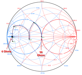
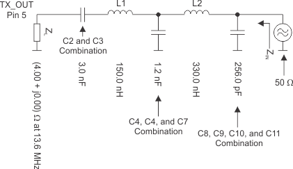
The output impedance of the TRF7970A when operated at full power out setting is nominally 4 + j0 (4 Ω real). This impedance must be matched to a resonant circuit and TI recommends matching circuit from 4 Ω to 50 Ω, as commercially available test equipment (for example, spectrum analyzers, power meters, and network analyzers) are 50-Ω systems. Figure 7-2 shows an impedance-matching reference circuit. Figure 7-3 shows a Smith chart simulation based on this circuit. This section explains how the values were calculated.
Starting with the 4-Ω source, the process of going from 4 Ω to 50 Ω can be represented on a Smith Chart simulator (available from http://www.fritz.dellsperger.net/). The elements are combined where appropriate (see Figure 7-2).
 Figure 7-3 Smith Chart Simulation
Resulting power out can be measured with a power meter or spectrum analyzer with power meter function or other equipment capable of making a "hot" measurement. Observe maximum power input levels on test equipment and use attenuators whenever available to avoid damage to equipment. Expected output power levels under various operating conditions are shown in Table 6-25.
