ZHCS363L August 2011 – March 2017 TRF7970A
PRODUCTION DATA.
- 1器件概述
- 2修订历史记录
- 3Device Characteristics
- 4Terminal Configuration and Functions
- 5Specifications
-
6Detailed Description
- 6.1 Overview
- 6.2 System Block Diagram
- 6.3 Power Supplies
- 6.4 Receiver – Analog Section
- 6.5 Receiver – Digital Section
- 6.6 Oscillator Section
- 6.7 Transmitter – Analog Section
- 6.8 Transmitter – Digital Section
- 6.9 Transmitter – External Power Amplifier and Subcarrier Detector
- 6.10 TRF7970A IC Communication Interface
- 6.11 TRF7970A Initialization
- 6.12 Special Direct Mode for Improved MIFARE Compatibility
- 6.13 NFC Modes
- 6.14
Direct Commands from MCU to Reader
- 6.14.1
Command Codes
- 6.14.1.1 Idle (0x00)
- 6.14.1.2 Software Initialization (0x03)
- 6.14.1.3 Initial RF Collision Avoidance (0x04)
- 6.14.1.4 Response RF Collision Avoidance (0x05)
- 6.14.1.5 Response RF Collision Avoidance (0x06, n = 0)
- 6.14.1.6 Reset FIFO (0x0F)
- 6.14.1.7 Transmission With CRC (0x11)
- 6.14.1.8 Transmission Without CRC (0x10)
- 6.14.1.9 Delayed Transmission With CRC (0x13)
- 6.14.1.10 Delayed Transmission Without CRC (0x12)
- 6.14.1.11 Transmit Next Time Slot (0x14)
- 6.14.1.12 Block Receiver (0x16)
- 6.14.1.13 Enable Receiver (0x17)
- 6.14.1.14 Test Internal RF (RSSI at RX Input With TX ON) (0x18)
- 6.14.1.15 Test External RF (RSSI at RX Input with TX OFF) (0x19)
- 6.14.1
Command Codes
- 6.15
Register Description
- 6.15.1 Register Preset
- 6.15.2 Register Overview
- 6.15.3
Detailed Register Description
- 6.15.3.1 Main Configuration Registers
- 6.15.3.2
Control Registers – Sublevel Configuration Registers
- 6.15.3.2.1 ISO/IEC 14443 TX Options Register (0x02)
- 6.15.3.2.2 ISO/IEC 14443 High-Bit-Rate and Parity Options Register (0x03)
- 6.15.3.2.3 TX Timer High Byte Control Register (0x04)
- 6.15.3.2.4 TX Timer Low Byte Control Register (0x05)
- 6.15.3.2.5 TX Pulse Length Control Register (0x06)
- 6.15.3.2.6 RX No Response Wait Time Register (0x07)
- 6.15.3.2.7 RX Wait Time Register (0x08)
- 6.15.3.2.8 Modulator and SYS_CLK Control Register (0x09)
- 6.15.3.2.9 RX Special Setting Register (0x0A)
- 6.15.3.2.10 Regulator and I/O Control Register (0x0B)
- 6.15.3.3
Status Registers
- 6.15.3.3.1 IRQ Status Register (0x0C)
- 6.15.3.3.2 Interrupt Mask Register (0x0D) and Collision Position Register (0x0E)
- 6.15.3.3.3 RSSI Levels and Oscillator Status Register (0x0F)
- 6.15.3.3.4 Special Functions Register (0x10)
- 6.15.3.3.5 Special Functions Register (0x11)
- 6.15.3.3.6 Adjustable FIFO IRQ Levels Register (0x14)
- 6.15.3.3.7 NFC Low Field Level Register (0x16)
- 6.15.3.3.8 NFCID1 Number Register (0x17)
- 6.15.3.3.9 NFC Target Detection Level Register (0x18)
- 6.15.3.3.10 NFC Target Protocol Register (0x19)
- 6.15.3.4 Test Registers
- 6.15.3.5 FIFO Control Registers
- 7Applications, Implementation, and Layout
- 8器件和文档支持
- 9机械、封装和可订购信息
6.1.1 RFID and NFC Operation – Reader and Writer
The TRF7970A is a high-performance 13.56-MHz HF RFID and NFC transceiver IC composed of an integrated analog front end (AFE) and a built-in data framing engine for ISO/IEC 15693, ISO/IEC 14443 A and B, and FeliCa. This includes data rates up to 848 kbps for ISO/IEC 14443 with all framing and synchronization tasks on board (in default mode). The TRF7970A also supports NFC tag type 1, 2, 3, 4, and 5 operations. This architecture lets the customer build a complete cost-effective yet high-performance multiprotocol 13.56-MHz RFID and NFC system together with a low-cost microcontroller.
Other standards and even custom protocols can be implemented by using either of the direct modes that the device offers. These direct modes (0 and 1) allow the user to fully control the analog front end (AFE) and also gain access to the raw subcarrier data or the unframed but already ISO formatted data and the associated (extracted) clock signal.
The receiver system has a dual input receiver architecture. The receivers also include various automatic and manual gain control options. The received input bandwidth can be selected to cover a broad range of input subcarrier signal options.
The received signal strength from transponders, ambient sources, or internal levels is available through the RSSI register. The receiver output is selectable among a digitized subcarrier signal and any of the integrated subcarrier decoders. The selected subcarrier decoder delivers the data bit stream and the data clock as outputs.
The TRF7970A also includes a receiver framing engine. This receiver framing engine performs the CRC or parity check, removes the EOF and SOF settings, and organizes the data in bytes for ISO/IEC 14443 A and B, ISO/IEC 15693, and FeliCa protocols. Framed data is then accessible to the microcontroller (MCU) through a 127-byte FIFO register.
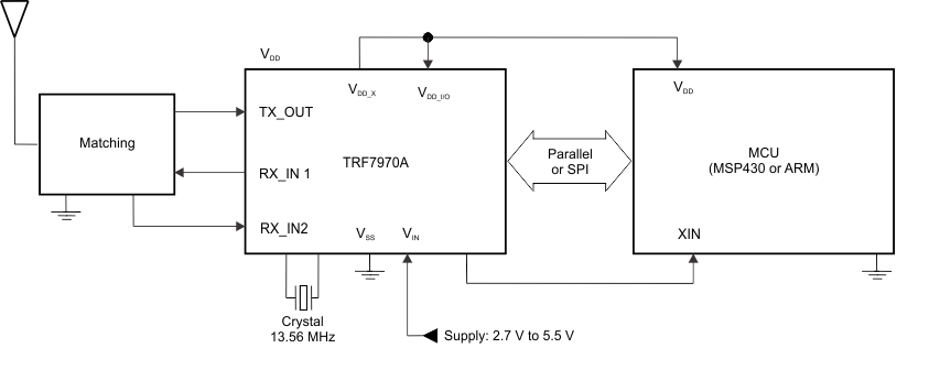
 Figure 6-1 Application Block Diagram
A parallel or serial interface (SPI) can be used for the communication between the MCU and the TRF7970A reader. When the built-in hardware encoders and decoders are used, transmit and receive functions use a 127-byte FIFO register. For direct transmit or receive functions, the encoders and decoders can be bypassed so that the MCU can process the data in real time. The TRF7970A supports data communication voltage levels from 1.8 V to 5.5 V for the MCU I/O interface. The transmitter has selectable output-power levels of 100 mW (+20 dBm) or 200 mW (+23 dBm) equivalent into a 50-Ω load when using a 5-V supply.
The transmitter supports OOK and ASK modulation with selectable modulation depth. The TRF7970A also includes a data transmission engine that comprises low-level encoding for ISO/IEC 15693, ISO/IEC 14443 A and B, and FeliCa. Included with the transmit data coding is the automatic generation of Start Of Frame (SOF), End Of Frame (EOF), Cyclic Redundancy Check (CRC), and parity bits.
Several integrated voltage regulators ensure a proper power-supply noise rejection for the complete reader system. The built-in programmable auxiliary voltage regulator VDD_X (pin 32), is able to deliver up to 20 mA to supply a microcontroller and additional external circuits within the reader system.