ZHCS363L August 2011 – March 2017 TRF7970A
PRODUCTION DATA.
- 1器件概述
- 2修订历史记录
- 3Device Characteristics
- 4Terminal Configuration and Functions
- 5Specifications
-
6Detailed Description
- 6.1 Overview
- 6.2 System Block Diagram
- 6.3 Power Supplies
- 6.4 Receiver – Analog Section
- 6.5 Receiver – Digital Section
- 6.6 Oscillator Section
- 6.7 Transmitter – Analog Section
- 6.8 Transmitter – Digital Section
- 6.9 Transmitter – External Power Amplifier and Subcarrier Detector
- 6.10 TRF7970A IC Communication Interface
- 6.11 TRF7970A Initialization
- 6.12 Special Direct Mode for Improved MIFARE Compatibility
- 6.13 NFC Modes
- 6.14
Direct Commands from MCU to Reader
- 6.14.1
Command Codes
- 6.14.1.1 Idle (0x00)
- 6.14.1.2 Software Initialization (0x03)
- 6.14.1.3 Initial RF Collision Avoidance (0x04)
- 6.14.1.4 Response RF Collision Avoidance (0x05)
- 6.14.1.5 Response RF Collision Avoidance (0x06, n = 0)
- 6.14.1.6 Reset FIFO (0x0F)
- 6.14.1.7 Transmission With CRC (0x11)
- 6.14.1.8 Transmission Without CRC (0x10)
- 6.14.1.9 Delayed Transmission With CRC (0x13)
- 6.14.1.10 Delayed Transmission Without CRC (0x12)
- 6.14.1.11 Transmit Next Time Slot (0x14)
- 6.14.1.12 Block Receiver (0x16)
- 6.14.1.13 Enable Receiver (0x17)
- 6.14.1.14 Test Internal RF (RSSI at RX Input With TX ON) (0x18)
- 6.14.1.15 Test External RF (RSSI at RX Input with TX OFF) (0x19)
- 6.14.1
Command Codes
- 6.15
Register Description
- 6.15.1 Register Preset
- 6.15.2 Register Overview
- 6.15.3
Detailed Register Description
- 6.15.3.1 Main Configuration Registers
- 6.15.3.2
Control Registers – Sublevel Configuration Registers
- 6.15.3.2.1 ISO/IEC 14443 TX Options Register (0x02)
- 6.15.3.2.2 ISO/IEC 14443 High-Bit-Rate and Parity Options Register (0x03)
- 6.15.3.2.3 TX Timer High Byte Control Register (0x04)
- 6.15.3.2.4 TX Timer Low Byte Control Register (0x05)
- 6.15.3.2.5 TX Pulse Length Control Register (0x06)
- 6.15.3.2.6 RX No Response Wait Time Register (0x07)
- 6.15.3.2.7 RX Wait Time Register (0x08)
- 6.15.3.2.8 Modulator and SYS_CLK Control Register (0x09)
- 6.15.3.2.9 RX Special Setting Register (0x0A)
- 6.15.3.2.10 Regulator and I/O Control Register (0x0B)
- 6.15.3.3
Status Registers
- 6.15.3.3.1 IRQ Status Register (0x0C)
- 6.15.3.3.2 Interrupt Mask Register (0x0D) and Collision Position Register (0x0E)
- 6.15.3.3.3 RSSI Levels and Oscillator Status Register (0x0F)
- 6.15.3.3.4 Special Functions Register (0x10)
- 6.15.3.3.5 Special Functions Register (0x11)
- 6.15.3.3.6 Adjustable FIFO IRQ Levels Register (0x14)
- 6.15.3.3.7 NFC Low Field Level Register (0x16)
- 6.15.3.3.8 NFCID1 Number Register (0x17)
- 6.15.3.3.9 NFC Target Detection Level Register (0x18)
- 6.15.3.3.10 NFC Target Protocol Register (0x19)
- 6.15.3.4 Test Registers
- 6.15.3.5 FIFO Control Registers
- 7Applications, Implementation, and Layout
- 8器件和文档支持
- 9机械、封装和可订购信息
6.3.3 Power Modes
The chip has several power states, which are controlled by two input pins (EN and EN2) and several bits in the chip status control register (0x00) (see Table 6-3 and Table 6-4).
Table 6-3 3.3-V Operation Power Modes(1)
| MODE | EN2 | EN | CHIP STATUS CONTROL REGISTER (0x00) | REGULATOR CONTROL REGISTER (0x0B) | TRANSMITTER | RECEIVER | SYS_CLK (13.56 MHz) | SYS_CLK (60 kHz) | VDD_X | TYPICAL CURRENT (mA) | TYPICAL POWER OUT (dBm) |
|---|---|---|---|---|---|---|---|---|---|---|---|
| Power down | 0 | 0 | XX | XX | OFF | OFF | OFF | OFF | OFF | <0.001 | - |
| Sleep mode | 1 | 0 | XX | XX | OFF | OFF | OFF | ON | ON | 0.120 | - |
| Standby mode at +3.3 VDC | X | 1 | 80 | 00 | OFF | OFF | ON | X | ON | 2 | - |
| Mode 1 at +3.3 VDC | X | 1 | 00 | 00 | OFF | OFF | ON | X | ON | 3 | - |
| Mode 2 at +3.3 VDC | X | 1 | 02 | 00 | OFF | ON | ON | X | ON | 9 | - |
| Mode 3 (half power) at +3.3 VDC | X | 1 | 30 | 07 | ON | ON | ON | X | ON | 53 | 14.5 |
| Mode 4 (full power) at +3.3 VDC | X | 1 | 20 | 07 | ON | ON | ON | X | ON | 67 | 17 |
Table 6-4 5-V Operation Power Modes(1)
| MODE | EN2 | EN | CHIP STATUS CONTROL REGISTER (0x00) | REGULATOR CONTROL REGISTER (0x0B) | TRANSMITTER | RECEIVER | SYS_CLK (13.56 MHz) | SYS_CLK (60 kHz) | VDD_X | TYPICAL CURRENT (mA) | TYPICAL POWER OUT (dBm) |
|---|---|---|---|---|---|---|---|---|---|---|---|
| Power down | 0 | 0 | XX | XX | OFF | OFF | OFF | OFF | OFF | <0.001 | - |
| Sleep mode | 1 | 0 | XX | XX | OFF | OFF | OFF | ON | ON | 0.120 | - |
| Standby mode at +5 VDC | X | 1 | 81 | 07 | OFF | OFF | ON | X | ON | 3 | - |
| Mode 1 at +5 VDC | X | 1 | 01 | 07 | OFF | OFF | ON | X | ON | 5 | - |
| Mode 2 at +5 VDC | X | 1 | 03 | 07 | OFF | ON | ON | X | ON | 10.5 | - |
| Mode 3 (half power) at +5 VDC | X | 1 | 31 | 07 | ON | ON | ON | X | ON | 70 | 20 |
| Mode 4 (full power) at +5 VDC | X | 1 | 21 | 07 | ON | ON | ON | X | ON | 130 | 23 |
Table 6-3 and Table 6-4 show the configuration for the different power modes when using a 3.3-V or 5-V system supply, respectively. The main reader enable signal is pin EN. When EN is set high, all of the reader regulators are enabled, the 13.56-MHz oscillator is running and the SYS_CLK (output clock for external microcontroller) is also available.
The input pin EN2 has two functions:
- A direct connection from EN2 to VIN to ensure the availability of the regulated supply VDD_X and an auxiliary clock signal (60 kHz, SYS_CLK) for an external MCU. This mode (EN = 0, EN2 = 1) is intended for systems in which the MCU is also being supplied by the reader supply regulator (VDD_X) and the MCU clock is supplied by the SYS_CLK output of the reader. This allows the MCU supply and clock to be available during sleep mode.
- EN2 enables the start-up of the reader system from complete power down (EN = 0, EN2 = 0). In this case the EN input is being controlled by the MCU (or other system device) that is without supply voltage during complete power down (thus unable to control the EN input). A rising edge applied to the EN2 input (which has an approximately 1-V threshold level) starts the reader supply system and 13.56-MHz oscillator (identical to condition EN = 1).
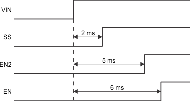
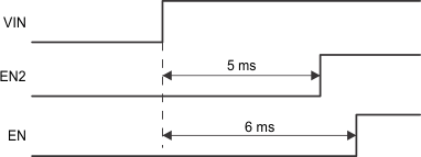
When user MCU is controlling EN and EN2, a delay of 1 ms between EN and EN2 must be used. If the MCU controls only EN, TI recommends connecting EN2 to either VIN or GND, depending on the application MCU requirements for VDD_X and SYS_CLK.
This start-up mode lasts until all of the regulators have settled and the 13.56-MHz oscillator has stabilized. If the EN input is set high (EN = 1) by the MCU (or other system device), the reader stays active. If the EN input is not set high (EN = 0) within 100 µs after the SYS_CLK output is switched from auxiliary clock (60 kHz) to high-frequency clock (derived from the crystal oscillator), the reader system returns to complete Power-Down Mode 1. This option can be used to wake-up the reader system from complete Power Down (PD Mode 1) by using a pushbutton switch or by sending a single pulse.
After the reader EN line is high, the other power modes are selected by control bits within the chip status control register (0x00). The power mode options and states are listed in Table 6-3.
When EN is set high (or on rising edge of EN2 and then confirmed by EN = 1) the supply regulators are activated and the 13.56-MHz oscillator is started. When the supplies are settled and the oscillator frequency is stable, the SYS_CLK output is switched from the auxiliary frequency of 60 kHz to the 13.56-MHz frequency derived from the crystal oscillator. At this point, the reader is ready to communicate and perform the required tasks. When this occurs, osc_ok (B6) of the RSSI Level and Oscillator Status register is set. The MCU can then program the Chip Status Control register 0x00 and select the operation mode by programming the additional registers.
- Standby Mode (bit 7 = 1 of register 0x00), the reader is capable of recovering to full operation in 100 µs.
- Mode 1 (active mode with RF output disabled, bit 5 = 0 and bit 1 = 0 of register 0x00) is a low power mode which allows the reader to recover to full operation within 25 µs.
- Mode 2 (active mode with only the RF receiver active, bit 1 = 1 of register 0x00) can be used to measure the external RF field (as described in RSSI measurements paragraph) if reader-to-reader anticollision is implemented.
- Modes 3 and 4 (active modes with the entire RF section active, bit 5 = 1 of register 0x00) are the normal modes used for normal transmit and receive operations.

