ZHCS363L August 2011 – March 2017 TRF7970A
PRODUCTION DATA.
- 1器件概述
- 2修订历史记录
- 3Device Characteristics
- 4Terminal Configuration and Functions
- 5Specifications
-
6Detailed Description
- 6.1 Overview
- 6.2 System Block Diagram
- 6.3 Power Supplies
- 6.4 Receiver – Analog Section
- 6.5 Receiver – Digital Section
- 6.6 Oscillator Section
- 6.7 Transmitter – Analog Section
- 6.8 Transmitter – Digital Section
- 6.9 Transmitter – External Power Amplifier and Subcarrier Detector
- 6.10 TRF7970A IC Communication Interface
- 6.11 TRF7970A Initialization
- 6.12 Special Direct Mode for Improved MIFARE Compatibility
- 6.13 NFC Modes
- 6.14
Direct Commands from MCU to Reader
- 6.14.1
Command Codes
- 6.14.1.1 Idle (0x00)
- 6.14.1.2 Software Initialization (0x03)
- 6.14.1.3 Initial RF Collision Avoidance (0x04)
- 6.14.1.4 Response RF Collision Avoidance (0x05)
- 6.14.1.5 Response RF Collision Avoidance (0x06, n = 0)
- 6.14.1.6 Reset FIFO (0x0F)
- 6.14.1.7 Transmission With CRC (0x11)
- 6.14.1.8 Transmission Without CRC (0x10)
- 6.14.1.9 Delayed Transmission With CRC (0x13)
- 6.14.1.10 Delayed Transmission Without CRC (0x12)
- 6.14.1.11 Transmit Next Time Slot (0x14)
- 6.14.1.12 Block Receiver (0x16)
- 6.14.1.13 Enable Receiver (0x17)
- 6.14.1.14 Test Internal RF (RSSI at RX Input With TX ON) (0x18)
- 6.14.1.15 Test External RF (RSSI at RX Input with TX OFF) (0x19)
- 6.14.1
Command Codes
- 6.15
Register Description
- 6.15.1 Register Preset
- 6.15.2 Register Overview
- 6.15.3
Detailed Register Description
- 6.15.3.1 Main Configuration Registers
- 6.15.3.2
Control Registers – Sublevel Configuration Registers
- 6.15.3.2.1 ISO/IEC 14443 TX Options Register (0x02)
- 6.15.3.2.2 ISO/IEC 14443 High-Bit-Rate and Parity Options Register (0x03)
- 6.15.3.2.3 TX Timer High Byte Control Register (0x04)
- 6.15.3.2.4 TX Timer Low Byte Control Register (0x05)
- 6.15.3.2.5 TX Pulse Length Control Register (0x06)
- 6.15.3.2.6 RX No Response Wait Time Register (0x07)
- 6.15.3.2.7 RX Wait Time Register (0x08)
- 6.15.3.2.8 Modulator and SYS_CLK Control Register (0x09)
- 6.15.3.2.9 RX Special Setting Register (0x0A)
- 6.15.3.2.10 Regulator and I/O Control Register (0x0B)
- 6.15.3.3
Status Registers
- 6.15.3.3.1 IRQ Status Register (0x0C)
- 6.15.3.3.2 Interrupt Mask Register (0x0D) and Collision Position Register (0x0E)
- 6.15.3.3.3 RSSI Levels and Oscillator Status Register (0x0F)
- 6.15.3.3.4 Special Functions Register (0x10)
- 6.15.3.3.5 Special Functions Register (0x11)
- 6.15.3.3.6 Adjustable FIFO IRQ Levels Register (0x14)
- 6.15.3.3.7 NFC Low Field Level Register (0x16)
- 6.15.3.3.8 NFCID1 Number Register (0x17)
- 6.15.3.3.9 NFC Target Detection Level Register (0x18)
- 6.15.3.3.10 NFC Target Protocol Register (0x19)
- 6.15.3.4 Test Registers
- 6.15.3.5 FIFO Control Registers
- 7Applications, Implementation, and Layout
- 8器件和文档支持
- 9机械、封装和可订购信息
6.10.1.4 FIFO Operation
The FIFO is a 127-byte register at address 0x1F with byte storage locations 0 to 126. FIFO data is loaded in a cyclical manner and can be cleared by a reset command (0x0F) (see Figure 6-12 showing this direct command).
Associated with the FIFO are two counters and three FIFO status flags. The first counter is a 7-bit FIFO byte counter (bits B0 to B6 in register 0x1C) that tracks the number of bytes loaded into the FIFO. If the number of bytes in the FIFO is n, the register value is n (number of bytes in FIFO register). For example, if 8 bytes are in the FIFO, the FIFO counter (Register 0x1C) has the hexadecimal value of 0x08 (binary value of 00001000).
A second counter (12 bits wide) indicates the number of bytes being transmitted (registers 0x1D and 0x1E) in a data frame. An extension to the transmission-byte counter is a 4-bit broken-byte counter also provided in register 0x1E (bits B0 to B3). Together these counters make up the TX length value that determines when the reader generates the EOF byte.
During transmission, the FIFO is checked for an almost-empty condition, and during reception for an almost-full condition. The maximum number of bytes that can be loaded into the FIFO in a single sequence is 127 bytes.
NOTE
The number of bytes in a frame, transmitted or received, can be greater than 127 bytes.
During transmission, the MCU loads the TRF7970A FIFO (or during reception the MCU removes data from the FIFO), and the FIFO counter counts the number of bytes being loaded into the FIFO. Meanwhile, the byte counter keeps track of the number of bytes being transmitted. An interrupt request is generated if the number of bytes in the FIFO triggers the watermark levels, which are configured in the Adjustable FIFO IRQ Levels register (0x14). The default setting is for the interrupt to be triggered when receiving 124 bytes during RX or having 4 bytes remaining during TX. These watermark levels are used so that MCU can send new data or read the data as necessary. The MCU must also validate the number of data bytes to be sent, so as to not surpass the value defined in the TX Length Byte registers (0x1D and 0x1E). The MCU also signals the transmit logic when the last byte of data is sent or was removed from the FIFO during reception.
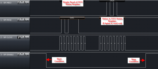
Figure 6-13 shows an example of checking the FIFO Status register using SPI with SS.
 Figure 6-13 Example of Checking the FIFO Status Register Using SPI With SS