ZHCS367E July 2011 – January 2016 ADS4249
PRODUCTION DATA.
- 1 特性
- 2 应用
- 3 说明
- 4 修订历史记录
- 5 ADS424x, ADS422x Family Comparison
- 6 Pin Configuration and Functions
-
7 Specifications
- 7.1 Absolute Maximum Ratings
- 7.2 ESD Ratings
- 7.3 Recommended Operating Conditions
- 7.4 Thermal Information
- 7.5 Electrical Characteristics: ADS4249 (250 MSPS)
- 7.6 Electrical Characteristics: General
- 7.7 Digital Characteristics
- 7.8 LVDS and CMOS Modes Timing Requirements
- 7.9 LVDS Timings at Lower Sampling Frequencies
- 7.10 CMOS Timings at Lower Sampling Frequencies
- 7.11 Serial Interface Timing Characteristics
- 7.12 Reset Timing (Only when Serial Interface is Used)
- 7.13 Typical Characteristics
-
8 Detailed Description
- 8.1 Overview
- 8.2 Functional Block Diagram
- 8.3 Feature Description
- 8.4 Device Functional Modes
- 8.5 Programming
- 8.6
Register Maps
- 8.6.1 Serial Register Map
- 8.6.2
Description of Serial Registers
- 8.6.2.1 Register Address 00h (Default = 00h)
- 8.6.2.2 Register Address 01h (Default = 00h)
- 8.6.2.3 Register Address 01h (Default = 00h)
- 8.6.2.4 Register Address 25h (Default = 00h)
- 8.6.2.5 Register Address 29h (Default = 00h)
- 8.6.2.6 Register Address 2Bh (Default = 00h)
- 8.6.2.7 Register Address 3Dh (Default = 00h)
- 8.6.2.8 Register Address 3Fh (Default = 00h)
- 8.6.2.9 Register Address 40h (Default = 00h)
- 8.6.2.10 Register Address 41h (Default = 00h)
- 8.6.2.11 Register Address 42h (Default = 00h)
- 8.6.2.12 Register Address 45h (Default = 00h)
- 8.6.2.13 Register Address 4Ah (Default = 00h)
- 8.6.2.14 Register Address 58h (Default = 00h)
- 8.6.2.15 Register Address BFh (Default = 00h)
- 8.6.2.16 Register Address C1h (Default = 00h)
- 8.6.2.17 Register Address CFh (Default = 00h)
- 8.6.2.18 Register Address EFh (Default = 00h)
- 8.6.2.19 Register Address F1h (Default = 00h)
- 8.6.2.20 Register Address F2h (Default = 00h)
- 8.6.2.21 Register Address 2h (Default = 00h)
- 8.6.2.22 Register Address D5h (Default = 00h)
- 8.6.2.23 Register Address D7h (Default = 00h)
- 8.6.2.24 Register Address DBh (Default = 00h)
- 9 Application and Implementation
- 10Power Supply Recommendations
- 11Layout
- 12器件和文档支持
- 13机械、封装和可订购信息
8 Detailed Description
8.1 Overview
The ADS4249 belongs to TI's ultralow power family of dual-channel, 14-bit analog-to-digital converters (ADCs). High performance is maintained when reducing power for power sensitive applications. In addition to its low power and high performance, the ADS4249 has a number of digital features and operating modes to enable design flexibility.
8.2 Functional Block Diagram
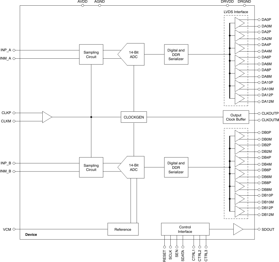
8.3 Feature Description
8.3.1 Digital Functions
The device has several useful digital functions (such as test patterns, gain, and offset correction). These functions require extra clock cycles for operation and increase the overall latency and power of the device. These digital functions are disabled by default after reset and the raw ADC output is routed to the output data pins with a latency of 16 clock cycles. Figure 37 shows more details of the processing after the ADC. In order to use any of the digital functions, the EN DIGITAL bit must be set to '1'. After this, the respective register bits must be programmed as described in the following sections and in the Serial Register Map section.
 Figure 37. Digital Processing Block
8.3.2 Gain for SFDR, SNR Trade-Off
The ADS4249 includes gain settings that can be used to get improved SFDR performance (compared to no gain). The gain is programmable from 0 dB to 6 dB (in 0.5-dB steps). For each gain setting, the analog input full-scale range scales proportionally, as shown in Table 2.
The SFDR improvement is achieved at the expense of SNR; for each gain setting, the SNR degrades approximately between 0.5 dB and 1 dB. The SNR degradation is reduced at high input frequencies. As a result, the gain is very useful at high input frequencies because the SFDR improvement is significant with marginal degradation in SNR. Therefore, the gain can be used as a trade-off between SFDR and SNR. Note that the default gain after reset is 0 dB.
Table 2. Full-Scale Range Across Gains
| GAIN (dB) | TYPE | FULL-SCALE (VPP) |
|---|---|---|
| 0 | Default after reset | 2 |
| 1 | Fine, programmable | 1.78 |
| 2 | Fine, programmable | 1.59 |
| 3 | Fine, programmable | 1.42 |
| 4 | Fine, programmable | 1.26 |
| 5 | Fine, programmable | 1.12 |
| 6 | Fine, programmable | 1 |
8.3.3 Offset Correction
The ADS4249 has an internal offset correction algorithm that estimates and corrects dc offset up to ±10 mV. The correction can be enabled using the ENABLE OFFSET CORR serial register bit. When enabled, the algorithm estimates the channel offset and applies the correction every clock cycle. The time constant of the correction loop is a function of the sampling clock frequency. The time constant can be controlled using the OFFSET CORR TIME CONSTANT register bits, as described in Table 3.
After the offset is estimated, the correction can be frozen by setting FREEZE OFFSET CORR = 0. When frozen, the last estimated value is used for the offset correction of every clock cycle. Note that offset correction is disabled by default after reset.
Table 3. Time Constant of Offset Correction Algorithm
| OFFSET CORR TIME CONSTANT | TIME CONSTANT, TCCLK
(Number of Clock Cycles) |
TIME CONSTANT, TCCLK × 1/fS (ms)(1) |
|---|---|---|
| 0000 | 1 M | 4 |
| 0001 | 2 M | 8 |
| 0010 | 4 M | 16 |
| 0011 | 8 M | 32 |
| 0100 | 16 M | 64 |
| 0101 | 32 M | 128 |
| 0110 | 64 M | 256 |
| 0111 | 128 M | 512 |
| 1000 | 256 M | 1024 |
| 1001 | 512 M | 2048 |
| 1010 | 1 G | 4096 |
| 1011 | 2 G | 8192 |
| 1100 | Reserved | — |
| 1101 | Reserved | — |
| 1110 | Reserved | — |
| 1111 | Reserved | — |
8.3.4 Power-Down
The ADS4249 has two power-down modes: global power-down and channel standby. These modes can be set using either the serial register bits or using the control pins CTRL1 to CTRL3 (as shown in Table 4).
Table 4. Power-Down Settings
| CTRL1 | CTRL2 | CTRL3 | DESCRIPTION |
|---|---|---|---|
| Low | Low | Low | Default |
| Low | Low | High | Not available |
| Low | High | Low | Not available |
| Low | High | High | Not available |
| High | Low | Low | Global power-down |
| High | Low | High | Channel A powered down, channel B is active |
| High | High | Low | Not available |
| High | High | High | MUX mode of operation, channel A and B data is multiplexed and output on DB[13:0] pins |
8.3.4.1 Global Power-Down
In this mode, the entire chip (including ADCs, internal reference, and output buffers) are powered down, resulting in reduced total power dissipation of approximately 20 mW when the CTRL pins are used and 3mW when the PDN GLOBAL serial register bit is used. The output buffers are in high-impedance state. The wake-up time from global power-down to data becoming valid in normal mode is typically 100 µs.
8.3.4.2 Channel Standby
In this mode, each ADC channel can be powered down. The internal references are active, resulting in a quick wake-up time of 50 µs. The total power dissipation in standby is approximately 240 mW at 250 MSPS.
8.3.4.3 Input Clock Stop
In addition to the previous modes, the converter enters a low-power mode when the input clock frequency falls below 1 MSPS. The power dissipation is approximately 160 mW.
8.3.5 Output Data Format
Two output data formats are supported: twos complement and offset binary. The format can be selected using the DATA FORMAT serial interface register bit or by controlling the DFS pin in parallel configuration mode.
In the event of an input voltage overdrive, the digital outputs go to the appropriate full-scale level. For a positive overdrive, the output code is 3FFFh for the ADS4249 in offset binary output format; the output code is 1FFFh for the ADS4249 in twos complement output format. For a negative input overdrive, the output code is 0000h in offset binary output format and 2000h for the ADS4249 in twos complement output format.
8.4 Device Functional Modes
8.4.1 Output Interface Modes
The ADS4249 provides 14-bit digital data for each channel and an output clock synchronized with the data.
8.4.1.1 Output Interface
Two output interface options are available: double data rate (DDR) LVDS and parallel CMOS. They can be selected using the serial interface register bit or by setting the proper voltage on the SEN pin in parallel configuration mode.
8.4.1.2 DDR LVDS Outputs
In this mode, the data bits and clock are output using low-voltage differential signal (LVDS) levels. Two data bits are multiplexed and output on each LVDS differential pair, as shown in Figure 38.
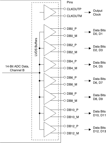 Figure 38. LVDS Interface
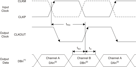
Even data bits (D0, D2, D4, and so forth) are output at the CLKOUTP rising edge and the odd data bits (D1, D3, D5, and so forth) are output at the CLKOUTP falling edge. Both the CLKOUTP rising and falling edges must be used to capture all the data bits, as shown in Figure 39.
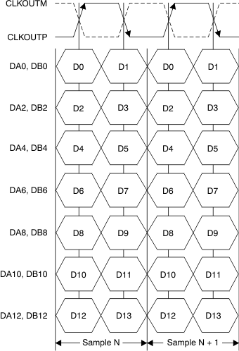 Figure 39. DDR LVDS Interface Timing
8.4.1.3 LVDS Buffer
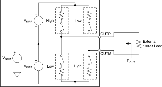
The equivalent circuit of each LVDS output buffer is shown in Figure 40. After reset, the buffer presents an output impedance of 100Ω to match with the external 100-Ω termination.
NOTE:
Default swing across 100-Ω load is ±350 mV. Use the LVDS SWING bits to change the swing.The VDIFF voltage is nominally 350 mV, resulting in an output swing of ±350 mV with 100-Ω external termination. The VDIFF voltage is programmable using the LVDS SWING register bits from ±125 mV to ±570 mV.
Additionally, a mode exists to double the strength of the LVDS buffer to support 50-Ω differential termination, as shown in Figure 41. This mode can be used when the output LVDS signal is routed to two separate receiver chips, each using a 100-Ω termination. The mode can be enabled using the LVDS DATA STRENGTH and LVDS CLKOUT STRENGTH register bits for data and output clock buffers, respectively.
The buffer output impedance behaves in the same way as a source-side series termination. Absorbing reflections from the receiver end helps improve signal integrity.
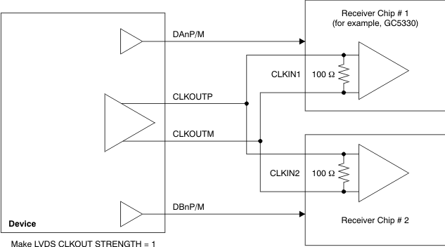 Figure 41. LVDS Buffer Differential Termination
8.4.1.4 Parallel CMOS Interface
In the CMOS mode, each data bit is output on separate pins as CMOS voltage level, every clock cycle, as Figure 42 shows. The rising edge of the output clock CLKOUT can be used to latch data in the receiver. Minimizing the load capacitance of the data and clock output pins is recommended by using short traces to the receiver. Furthermore, match the output data and clock traces to minimize the skew between them.
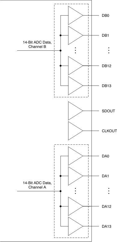 Figure 42. CMOS Outputs
8.4.1.5 CMOS Interface Power Dissipation
With CMOS outputs, the DRVDD current scales with the sampling frequency and the load capacitance on every output pin. The maximum DRVDD current occurs when each output bit toggles between 0 and 1 every clock cycle. In actual applications, this condition is unlikely to occur. The actual DRVDD current would be determined by the average number of output bits switching, which is a function of the sampling frequency and the nature of the analog input signal. This relationship is shown by Equation 1:
where
- CL = load capacitance,
- N × FAVG = average number of output bits switching.
8.4.1.6 Multiplexed Mode of Operation
In this mode, the digital outputs of both channels are multiplexed and output on a single bus (DB[11:0] pins), as shown in Figure 43. The channel A output pins (DA[11:0]) are in 3-state. Because the output data rate on the DB bus is effectively doubled, this mode is recommended only for low sampling frequencies (less than 80 MSPS). This mode can be enabled using the POWER-DOWN MODE register bits or using the CTRL[3:1] parallel pins.
8.5 Programming
The ADS4249 can be configured independently using either parallel interface control or serial interface programming. Table 5 lists the device high-performance modes.
Table 5. High-Performance Modes(1)(2)
| PARAMETER | DESCRIPTION |
|---|---|
| High-performance mode | Set the HIGH PERF MODE[2:1] register bit to obtain best performance across sample clock and input signal frequencies. Register address = 03h, data = 03h |
| High-frequency mode | Set the HIGH FREQ MODE CH A and HIGH FREQ MODE CH B register bits for high input signal frequencies greater than 200 MHz. Register address = 4Ah, data = 01h Register address = 58h, data = 01h |
| High-speed mode | Set the HIGH PERF MODE[8:3] bits to obtain best performance across input signal frequencies for sampling rates greater than 160 MSPS. Note that this mode changes VCM to 0.87 V from its default value of 0.95 V. Register address = 2h, data = 40h Register address = D5h, data = 18h Register address = D7h, data = 0Ch Register address = DBh, data = 20h |
8.5.1 Parallel Configuration Only
To put the device into parallel configuration mode, keep RESET tied high (AVDD). Then, use the SEN, SCLK, CTRL1, CTRL2, and CTRL3 pins to directly control certain modes of the ADC. The device can be easily configured by connecting the parallel pins to the correct voltage levels (as described in Table 6 to Table 9). There is no need to apply a reset and SDATA can be connected to ground.
In this mode, SEN and SCLK function as parallel interface control pins. Some frequently-used functions can be controlled using these pins. Table 6 describes the modes controlled by the parallel pins.
Table 6. Parallel Pin Definition
| PIN | CONTROL MODE |
|---|---|
| SCLK | Low-speed mode selection |
| SEN | Output data format and output interface selection |
| CTRL1 | Together, these pins control the power-down modes |
| CTRL2 | |
| CTRL3 |
8.5.2 Serial Interface Configuration Only
To enable this mode, the serial registers must first be reset to the default values and the RESET pin must be kept low. SEN, SDATA, and SCLK function as serial interface pins in this mode and can be used to access the internal registers of the ADC. The registers can be reset either by applying a pulse on the RESET pin or by setting the RESET bit high. The Serial Register Map section describes the register programming and the register reset process in more detail.
8.5.3 Using Both Serial Interface and Parallel Controls
For increased flexibility, a combination of serial interface registers and parallel pin controls (CTRL1 to CTRL3) can also be used to configure the device. To enable this option, keep RESET low. The parallel interface control pins CTRL1 to CTRL3 are available. After power-up, the device is automatically configured according to the voltage settings on these pins (see Table 9). SEN, SDATA, and SCLK function as serial interface digital pins and are used to access the internal registers of the ADC. The registers must first be reset to the default values either by applying a pulse on the RESET pin or by setting the RESET bit to '1'. After reset, the RESET pin must be kept low. The Serial Register Map section describes register programming and the register reset process in more detail.
8.5.4 Parallel Configuration Details
The functions controlled by each parallel pin are described in Table 7, Table 8, and Table 9. A simple way of configuring the parallel pins is shown in Figure 44.
Table 7. SCLK Control Pin
| VOLTAGE APPLIED ON SCLK | DESCRIPTION |
|---|---|
| Low | Low-speed mode is disabled |
| High | Low-speed mode is enabled |
Table 8. SEN Control Pin
| VOLTAGE APPLIED ON SEN | DESCRIPTION |
|---|---|
| 0 (50 mV / 0 mV) |
Twos complement and parallel CMOS output |
| (3/8) AVDD (±50 mV) |
Offset binary and parallel CMOS output |
| (5/8) 2AVDD (±5 0mV) |
Offset binary and DDR LVDS output |
| AVDD (0 mV / –50 mV) |
Twos complement and DDR LVDS output |
Table 9. CTRL1, CTRL2, and CTRL3 Pins
| CTRL1 | CTRL2 | CTRL3 | DESCRIPTION |
|---|---|---|---|
| Low | Low | Low | Normal operation |
| Low | Low | High | Not available |
| Low | High | Low | Not available |
| Low | High | High | Not available |
| High | Low | Low | Global power-down |
| High | Low | High | Channel A standby, channel B is active |
| High | High | Low | Not available |
| High | High | High | MUX mode of operation, channel A and B data are multiplexed and output on the DB[13:0] pins. See the Multiplexed Mode of Operation section for further details. |
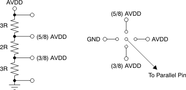 Figure 44. Simple Scheme to Configure the Parallel Pins
8.5.5 Serial Interface Details
The ADC has a set of internal registers that can be accessed by the serial interface formed by the SEN (serial interface enable), SCLK (serial interface clock), and SDATA (serial interface data) pins. Serial shift of bits into the device is enabled when SEN is low. Serial data SDATA are latched at every SCLK falling edge when SEN is active (low). The serial data are loaded into the register at every 16th SCLK falling edge when SEN is low. When the word length exceeds a multiple of 16 bits, the excess bits are ignored. Data can be loaded in multiples of 16-bit words within a single active SEN pulse. The first eight bits form the register address and the remaining eight bits are the register data. The interface can work with SCLK frequencies from 20 MHz down to very low speeds (of a few hertz) and also with non-50% SCLK duty cycle.
8.5.5.1 Register Initialization
After power-up, the internal registers must be initialized to the default values. Initialization can be accomplished in one of two ways:
- Through a hardware reset by applying a high pulse on the RESET pin (of durations greater than 10 ns), see Figure 5 and the Serial Interface Timing Characteristics table; or
- By applying a software reset. When using the serial interface, set the RESET bit high. This setting initializes the internal registers to the default values and then self-resets the RESET bit low. In this case, the RESET pin is kept low. See the Reset Timing (Only when Serial Interface is Used) section and Figure 6 for reset timing.
8.5.5.2 Serial Register Readout
The device includes a mode where the contents of the internal registers can be read back. This readback mode may be useful as a diagnostic check to verify the serial interface communication between the external controller and the ADC. To use readback mode, follow this procedure:
- Set the READOUT register bit to '1'. This setting disables any further writes to the registers.
- Initiate a serial interface cycle specifying the address of the register (A7 to A0) whose content has to be read.
- The device outputs the contents (D7 to D0) of the selected register on the SDOUT pin (pin 64).
- The external controller can latch the contents at the SCLK falling edge.
- To enable register writes, reset the READOUT register bit to '0'.
The serial register readout works with both CMOS and LVDS interfaces on pin 64. Figure 45 shows the serial readout timing diagram.
When READOUT is disabled, the SDOUT pin is in high-impedance state.
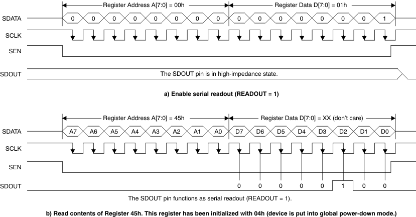 Figure 45. Serial Readout Timing Diagram
8.6 Register Maps
8.6.1 Serial Register Map
Table 10 summarizes the functions supported by the serial interface.
Table 10. Serial Interface Register Map(1)
8.6.2 Description of Serial Registers
8.6.2.1 Register Address 00h (Default = 00h)
| 7 | 6 | 5 | 4 | 3 | 2 | 1 | 0 |
| 0 | 0 | 0 | 0 | 0 | 0 | RESET | READOUT |
| Bits[7:2] | Always write '0' |
| Bit 1 | RESET: Software reset applied |
| This bit resets all internal registers to the default values and self-clears to 0 (default = 1). | |
| Bit 0 | READOUT: Serial readout |
| This bit sets the serial readout of the registers. 0 = Serial readout of registers disabled; the SDOUT pin is placed in a high-impedance state. 1 = Serial readout enabled; the SDOUT pin functions as a serial data readout with CMOS logic levels running from the DRVDD supply. See the Serial Register Readout section. |
8.6.2.2 Register Address 01h (Default = 00h)
| 7 | 6 | 5 | 4 | 3 | 2 | 1 | 0 |
| LVDS SWING | 0 | 0 | |||||
| Bits[7:2] | LVDS SWING: LVDS swing programmability |
| These bits program the LVDS swing. Set the EN LVDS SWING bit to '1' before programming swing. 000000 = Default LVDS swing; ±350 mV with external 100-Ω termination 011011 = LVDS swing ±410 mV 110010 = LVDS swing ±465 mV 010100 = LVDS swing ±570 mV 111110 = LVDS swing ±200 mV 001111 = LVDS swing ±125 mV |
|
| Bits[1:0] | Always write '0' |
8.6.2.3 Register Address 01h (Default = 00h)
| 7 | 6 | 5 | 4 | 3 | 2 | 1 | 0 |
| 0 | 0 | 0 | 0 | 0 | 0 | HIGH PERF MODE 2 | HIGH PERF MODE 1 |
| Bits[7:2] | Always write '0' |
| Bits[1:0] | HIGH PERF MODE[2:1]: High-performance mode |
| 00 = Default performance 01 = Do not use 10 = Do not use 11 = Obtain best performance across sample clock and input signal frequencies |
8.6.2.4 Register Address 25h (Default = 00h)
| 7 | 6 | 5 | 4 | 3 | 2 | 1 | 0 |
| CH A GAIN | 0 | CH A TEST PATTERNS | |||||
| Bits[7:4] | CH A GAIN: Channel A gain programmability | ||
| These bits set the gain programmability in 0.5-dB steps for channel A. | |||
| 0000 = 0-dB gain (default after reset) 0001 = 0.5-dB gain 0010 = 1-dB gain 0011 = 1.5-dB gain 0100 = 2-dB gain 0101 = 2.5-dB gain 0110 = 3-dB gain 0111 = 3.5-dB gain 1000 = 4-dB gain 1001 = 4.5-dB gain 1010 = 5-dB gain 1011 = 5.5-dB gain 1100 = 6-dB gain |
|||
| Bit 3 | Always write '0' | ||
| Bits[2:0] | CH A TEST PATTERNS: Channel A data capture | ||
| These bits verify data capture for channel A. 000 = Normal operation 001 = Outputs all 0s 010 = Outputs all 1s 011 = Outputs toggle pattern. The output data D[13:0] are an alternating sequence of 10101010101010 and 01010101010101. 100 = Outputs digital ramp. 101 = Outputs custom pattern; use registers 3Fh and 40h to set the custom pattern 110 = Unused 111 = Unused |
|||
8.6.2.5 Register Address 29h (Default = 00h)
| 7 | 6 | 5 | 4 | 3 | 2 | 1 | 0 |
| 0 | 0 | 0 | DATA FORMAT | 0 | 0 | 0 | |
| Bits[7:5] | Always write '0' | ||
| Bits[4:3] | DATA FORMAT: Data format selection | ||
| 00 = Twos complement 01 = Twos complement 10 = Twos complement 11 = Offset binary |
|||
| Bits[2:0] | Always write '0' | ||
8.6.2.6 Register Address 2Bh (Default = 00h)
| 7 | 6 | 5 | 4 | 3 | 2 | 1 | 0 |
| CH B GAIN | 0 | CH B TEST PATTERNS | |||||
| Bits[7:4] | CH B GAIN: Channel B gain programmability | ||
| These bits set the gain programmability in 0.5-dB steps for channel B. | |||
| 0000 = 0-dB gain (default after reset) 0001 = 0.5-dB gain 0010 = 1-dB gain 0011 = 1.5-dB gain 0100 = 2-dB gain 0101 = 2.5-dB gain 0110 = 3-dB gain 0111 = 3.5-dB gain 1000 = 4-dB gain 1001 = 4.5-dB gain 1010 = 5-dB gain 1011 = 5.5-dB gain 1100 = 6-dB gain |
|||
| Bit 3 | Always write '0' | ||
| Bits[2:0] | CH B TEST PATTERNS: Channel B data capture | ||
| These bits verify data capture for channel B. 000 = Normal operation 001 = Outputs all 0s 010 = Outputs all 1s 011 = Outputs toggle pattern. The output data D[13:0] are an alternating sequence of 10101010101010 and 01010101010101. 100 = Outputs digital ramp. 101 = Outputs custom pattern; use registers 3Fh and 40h to set the custom pattern 110 = Unused 111 = Unused |
|||
8.6.2.7 Register Address 3Dh (Default = 00h)
| 7 | 6 | 5 | 4 | 3 | 2 | 1 | 0 |
| 0 | 0 | ENABLE OFFSET CORR | 0 | 0 | 0 | 0 | 0 |
| Bits[7:6] | Always write '0' |
| Bit 5 | ENABLE OFFSET CORR: Offset correction setting |
| This bit enables the offset correction. 0 = Offset correction disabled 1 = Offset correction enabled |
|
| Bits[4:0] | Always write '0' |
8.6.2.8 Register Address 3Fh (Default = 00h)
| 7 | 6 | 5 | 4 | 3 | 2 | 1 | 0 |
| 0 | 0 | CUSTOM PATTERN D13 | CUSTOM PATTERN D12 | CUSTOM PATTERN D11 | CUSTOM PATTERN D10 | CUSTOM PATTERN D9 | CUSTOM PATTERN D8 |
| Bits[7:6] | Always write '0' |
| Bits[5:0] | CUSTOM PATTERN D[13:8] |
| These are the six upper bits of the custom pattern available at the output instead of ADC data. The ADS4249 custom pattern is 14-bit. |
8.6.2.9 Register Address 40h (Default = 00h)
| 7 | 6 | 5 | 4 | 3 | 2 | 1 | 0 |
| CUSTOM PATTERN D7 | CUSTOM PATTERN D6 | CUSTOM PATTERN D5 | CUSTOM PATTERN D4 | CUSTOM PATTERN D3 | CUSTOM PATTERN D2 | CUSTOM PATTERN D1 | CUSTOM PATTERN D0 |
| Bits[7:0] | CUSTOM PATTERN D[7:0] |
| These are the eight lower bits of the custom pattern available at the output instead of ADC data. The ADS4249 custom pattern is 14-bit; use the CUSTOM PATTERN D[13:0] register bits. |
8.6.2.10 Register Address 41h (Default = 00h)
| 7 | 6 | 5 | 4 | 3 | 2 | 1 | 0 |
| LVDS CMOS | CMOS CLKOUT STRENGTH | 0 | 0 | DIS OBUF | |||
| Bits[7:6] | LVDS CMOS: Interface selection |
| These bits select the interface. 00 = DDR LVDS interface 01 = DDR LVDS interface 10 = DDR LVDS interface 11 = Parallel CMOS interface |
|
| Bits[5:4] | CMOS CLKOUT STRENGTH |
| These bits control the strength of the CMOS output clock. 00 = Maximum strength (recommended) 01 = Medium strength 10 = Low strength 11 = Very low strength |
|
| Bits[3:2] | Always write '0' |
| Bits[1:0] | DIS OBUF |
| These bits power down data and clock output buffers for both the CMOS and LVDS output interface. When powered down, the output buffers are in 3-state. 00 = Default 01 = Power-down data output buffers for channel B 10 = Power-down data output buffers for channel A 11 = Power-down data output buffers for both channels as well as the clock output buffer |
8.6.2.11 Register Address 42h (Default = 00h)
| 7 | 6 | 5 | 4 | 3 | 2 | 1 | 0 |
| CLKOUT FALL POSN | CLKOUT RISE POSN | EN DIGITAL | 0 | 0 | 0 | ||
| Bits[7:6] | CLKOUT FALL POSN |
| In LVDS mode: 00 = Default 01 = The falling edge of the output clock advances by 450 ps 10 = The falling edge of the output clock advances by 150 ps 11 = The falling edge of the output clock is delayed by 550 ps In CMOS mode: 00 = Default 01 = The falling edge of the output clock is delayed by 150 ps 10 = Do not use 11 = The falling edge of the output clock advances by 100 ps |
|
| Bits[5:6] | CLKOUT RISE POSN |
| In LVDS mode: 00 = Default 01 = The rising edge of the output clock advances by 450 ps 10 = The rising edge of the output clock advances by 150 ps 11 = The rising edge of the output clock is delayed by 250 ps In CMOS mode: 00 = Default 01 = The rising edge of the output clock is delayed by 150 ps 10 = Do not use 11 = The rising edge of the output clock advances by 100 ps |
|
| Bit 3 | EN DIGITAL: Digital function enable |
| 0 = All digital functions disabled 1 = All digital functions (such as test patterns, gain, and offset correction) enabled |
|
| Bits[2:0] | Always write '0' |
8.6.2.12 Register Address 45h (Default = 00h)
| 7 | 6 | 5 | 4 | 3 | 2 | 1 | 0 |
| STBY | LVDS CLKOUT STRENGTH | LVDS DATA STRENGTH | 0 | 0 | PDN GLOBAL | 0 | 0 |
| Bit 7 | STBY: Standby setting | ||
| 0 = Normal operation 1 = Both channels are put in standby; wakeup time from this mode is fast (typically 50 µs). |
|||
| Bit 6 | LVDS CLKOUT STRENGTH: LVDS output clock buffer strength setting | ||
| 0 = LVDS output clock buffer at default strength to be used with 100-Ω external termination 1 = LVDS output clock buffer has double strength to be used with 50-Ω external termination |
|||
| Bit 5 | LVDS DATA STRENGTH | ||
| 0 = All LVDS data buffers at default strength to be used with 100-Ω external termination 1 = All LVDS data buffers have double strength to be used with 50-Ω external termination |
|||
| Bits[4:3] | Always write '0' | ||
| Bit 2 | PDN GLOBAL | ||
| 0 = Normal operation 1 = Total power down; all ADC channels, internal references, and output buffers are powered down. Wakeup time from this mode is slow (typically 100 µs). |
|||
| Bits[1:0] | Always write '0' | ||
8.6.2.13 Register Address 4Ah (Default = 00h)
| 7 | 6 | 5 | 4 | 3 | 2 | 1 | 0 |
| 0 | 0 | 0 | 0 | 0 | 0 | 0 | HIGH FREQ MODE CH B |
| Bits[7:1] | Always write '0' | ||
| Bit 0 | HIGH FREQ MODE CH B: High-frequency mode for channel B | ||
| 0 = Default 1 = Use this mode for high input frequencies greater than 200 MHz |
|||
8.6.2.14 Register Address 58h (Default = 00h)
| 7 | 6 | 5 | 4 | 3 | 2 | 1 | 0 |
| 0 | 0 | 0 | 0 | 0 | 0 | 0 | HIGH FREQ MODE CH A |
| Bits[7:1] | Always write '0' | ||
| Bit 0 | HIGH FREQ MODE CH A: High-frequency mode for channel A | ||
| 0 = Default 1 = Use this mode for high input frequencies greater than 200 MHz |
|||
8.6.2.15 Register Address BFh (Default = 00h)
| 7 | 6 | 5 | 4 | 3 | 2 | 1 | 0 |
| CH A OFFSET PEDESTAL | 0 | 0 | |||||
| Bits[7:4] | CH A OFFSET PEDESTAL: Channel A offset pedestal selection | ||
| When the offset correction is enabled, the final converged value after the offset is corrected is the ADC midcode value. A pedestal can be added to the final converged value by programming these bits. See the Offset Correction section. Channels can be independently programmed for different offset pedestals by choosing the relevant register address. The pedestal ranges from –32 to +31, so the output code can vary from midcode-32 to midcode+31 by adding pedestal D7-D2. |
|||
| Program bits D[7:2] | |||
| 011111 = Midcode+31 011110 = Midcode+30 011101 = Midcode+29 … 000010 = Midcode+2 000001 = Midcode+1 000000 = Midcode 111111 = Midcode-1 111110 = Midcode-2 … 100000 = Midcode-32 |
|||
| Bits[3:0] | Always write '0' | ||
8.6.2.16 Register Address C1h (Default = 00h)
| 7 | 6 | 5 | 4 | 3 | 2 | 1 | 0 |
| CH B OFFSET PEDESTAL | 0 | 0 | |||||
| Bits[7:4] | CH B OFFSET PEDESTAL: Channel B offset pedestal selection | |
| When offset correction is enabled, the final converged value after the offset is corrected is the ADC midcode value. A pedestal can be added to the final converged value by programming these bits; see the Offset Correction section. Channels can be independently programmed for different offset pedestals by choosing the relevant register address. The pedestal ranges from –32 to +31, so the output code can vary from midcode-32 to midcode+31 by adding pedestal D7-D2. |
||
| Program Bits D[7:2] | ||
| 011111 = Midcode+31 011110 = Midcode+30 011101 = Midcode+29 … 000010 = Midcode+2 000001 = Midcode+1 000000 = Midcode 111111 = Midcode-1 111110 = Midcode-2 … 100000 = Midcode-32 |
||
| Bits[3:0] | Always write '0' | |
8.6.2.17 Register Address CFh (Default = 00h)
| 7 | 6 | 5 | 4 | 3 | 2 | 1 | 0 |
| FREEZE OFFSET CORR | 0 | OFFSET CORR TIME CONSTANT | 0 | 0 | |||
| Bit 7 | FREEZE OFFSET CORR: Freeze offset correction setting | |
| This bit sets the freeze offset correction estimation. 0 = Estimation of offset correction is not frozen (the EN OFFSET CORR bit must be set) 1 = Estimation of offset correction is frozen (the EN OFFSET CORR bit must be set); when frozen, the last estimated value is used for offset correction of every clock cycle. See the Offset Correction section. |
||
| Bit 6 | Always write '0' | |
| Bits[5:2] | OFFSET CORR TIME CONSTANT | |
| The offset correction loop time constant in number of clock cycles. See the Offset Correction section. | ||
| Bits[1:0] | Always write '0' | |
8.6.2.18 Register Address EFh (Default = 00h)
| 7 | 6 | 5 | 4 | 3 | 2 | 1 | 0 |
| 0 | 0 | 0 | EN LOW SPEED MODE | 0 | 0 | 0 | 0 |
| Bits[7:5] | Always write '0' |
| Bit 4 | EN LOW SPEED MODE: Enable control of low-speed mode through serial register bits |
| This bit enables the control of the low-speed mode using the LOW SPEED MODE CH B and LOW SPEED MODE CH A register bits. 0 = Low-speed mode is disabled 1 = Low-speed mode is controlled by serial register bits |
|
| Bits[3:0] | Always write '0' |
8.6.2.19 Register Address F1h (Default = 00h)
| 7 | 6 | 5 | 4 | 3 | 2 | 1 | 0 |
| 0 | 0 | 0 | 0 | 0 | 0 | EN LVDS SWING | |
| Bits[7:2] | Always write '0' |
| Bits[1:0] | EN LVDS SWING: LVDS swing enable |
| These bits enable LVDS swing control using the LVDS SWING register bits. 00 = LVDS swing control using the LVDS SWING register bits is disabled 01 = Do not use 10 = Do not use 11 = LVDS swing control using the LVDS SWING register bits is enabled |
8.6.2.20 Register Address F2h (Default = 00h)
| 7 | 6 | 5 | 4 | 3 | 2 | 1 | 0 |
| 0 | 0 | 0 | 0 | LOW SPEED MODE CH A | 0 | 0 | 0 |
| Bits[7:4] | Always write '0' |
| Bit 3 | LOW SPEED MODE CH A: Channel A low-speed mode enable |
| This bit enables the low-speed mode for channel A. Set the EN LOW SPEED MODE bit to '1' before using this bit. 0 = Low-speed mode is disabled for channel A 1 = Low-speed mode is enabled for channel A |
|
| Bits[2:0] | Always write '0' |
8.6.2.21 Register Address 2h (Default = 00h)
| 7 | 6 | 5 | 4 | 3 | 2 | 1 | 0 |
| 0 | HIGH PERF MODE3 | 0 | 0 | 0 | 0 | 0 | 0 |
| Bit 7 | Always write '0' |
| Bit 6 | HIGH PERF MODE3 |
| HIGH PERF MODE3 to HIGH PERF MODE8 must be set to '1' to ensure best performance at high sampling speed (greater than 160 MSPS) | |
| Bits[5:0] | Always write '0' |
8.6.2.22 Register Address D5h (Default = 00h)
| 7 | 6 | 5 | 4 | 3 | 2 | 1 | 0 |
| 0 | 0 | 0 | HIGH PERF MODE4 | HIGH PERF MODE5 | 0 | 0 | 0 |
| Bits[7:5] | Always write '0' |
| Bit 4 | HIGH PERF MODE4 |
| HIGH PERF MODE3 to HIGH PERF MODE8 must be set to '1' to ensure best performance at high sampling speed (greater than 160 MSPS) | |
| Bit 3 | HIGH PERF MODE5 |
| HIGH PERF MODE3 to HIGH PERF MODE8 must be set to '1' to ensure best performance at high sampling speed (greater than 160 MSPS) | |
| Bits[2:0] | Always write '0' |
8.6.2.23 Register Address D7h (Default = 00h)
| 7 | 6 | 5 | 4 | 3 | 2 | 1 | 0 |
| 0 | 0 | 0 | 0 | HIGH PERF MODE6 | HIGH PERF MODE7 | 0 | 0 |
| Bits[7:4] | Always write '0' |
| Bit 3 | HIGH PERF MODE6 |
| HIGH PERF MODE3 to HIGH PERF MODE8 must be set to '1' to ensure best performance at high sampling speed (greater than 160 MSPS) | |
| Bit 2 | HIGH PERF MODE7 |
| HIGH PERF MODE3 to HIGH PERF MODE8 must be set to '1' to ensure best performance at high sampling speed (greater than 160 MSPS) | |
| Bits[1:0] | Always write '0' |
8.6.2.24 Register Address DBh (Default = 00h)
| 7 | 6 | 5 | 4 | 3 | 2 | 1 | 0 |
| 0 | 0 | HIGH PERF MODE8 | 0 | 0 | 0 | 0 | LOW SPEED MODE CH B |
| Bits[7:6] | Always write '0' |
| Bit 5 | HIGH PERF MODE8 |
| HIGH PERF MODE3 to HIGH PERF MODE8 must be set to '1' to ensure best performance at high sampling speed (greater than 160 MSPS). | |
| Bits[4:1] | Always write '0' |
| Bit 0 | LOW SPEED MODE CH B: Channel B low-speed mode enable |
| This bit enables the low-speed mode for channel B. Set the EN LOW SPEED MODE bit to '1' before using this bit. 0 = Low-speed mode is disabled for channel B 1 = Low-speed mode is enabled for channel B |