ZHCS404F September 2011 – October 2015 TPD12S016
PRODUCTION DATA.
- 1 特性
- 2 应用范围
- 3 说明
- 4 修订历史记录
- 5 Pin Configuration and Functions
- 6 Specifications
-
7 Detailed Description
- 7.1 Overview
- 7.2 Functional Block Diagram
- 7.3
Feature Description
- 7.3.1 Conforms to HDMI Compliance Tests Without any External Components
- 7.3.2 IEC 61000-4-2 ESD Protection
- 7.3.3 Supports HDMI 1.4 Data Rate
- 7.3.4 Matches Class D and Class C Pin Mapping
- 7.3.5 8-Channel ESD Lines for Four Differential Pairs with Ultra-low Differential Capacitance Matching (0.05 pF)
- 7.3.6 On-Chip Load Switch With 55-mA Current Limit Feature at the HDMI 5V_OUT Pin
- 7.3.7 Auto-direction Sensing I2C Level Shifter With One-Shot Circuit to Drive a Long HDMI Cable (750-pF Load)
- 7.3.8 Back-Drive Protection on HDMI Connector Side Ports
- 7.3.9 Integrated Pullup and Pulldown Resistors per HDMI Specification
- 7.3.10 Space Saving 24-Pin RKT Package and 24-TSSOP Package
- 7.3.11 DDC/CEC LEVEL SHIFT Circuit Operation
- 7.3.12 DDC/CEC Level Shifter Operational Notes For VCCA = 1.8 V
- 7.3.13 Rise-Time Accelerators
- 7.3.14 Noise Considerations
- 7.3.15 Resistor Pullup Value Selection
- 7.4 Device Functional Modes
- 8 Application and Implementation
- 9 Power Supply Recommendations
- 10Layout
- 11器件和文档支持
- 12机械、封装和可订购信息
10 Layout
10.1 Layout Guidelines
- The optimum placement is as close to the connector as possible.
- EMI during an ESD event can couple from the trace being struck to other nearby unprotected traces, resulting in early system failures. Therefore, the PCB designer needs to minimize the possibility of EMI coupling by keeping any unprotected traces away from the protected traces which are between the TVS and the connector.
- Route the protected traces as straight as possible.
- Avoid using VIAs between the connecter and an I/O protection pin on TPD12S016.
- Avoid 90º turns in traces.
- Electric fields tend to build up on corners, increasing EMI coupling.
- Minimize impedance on the path to GND for maximum ESD dissipation.
- The capacitors on VBUS and VOTG_IN should be placed close to their respective pins on TPD12S016.
10.2 Layout Examples
10.2.1 TPD12S016RKT
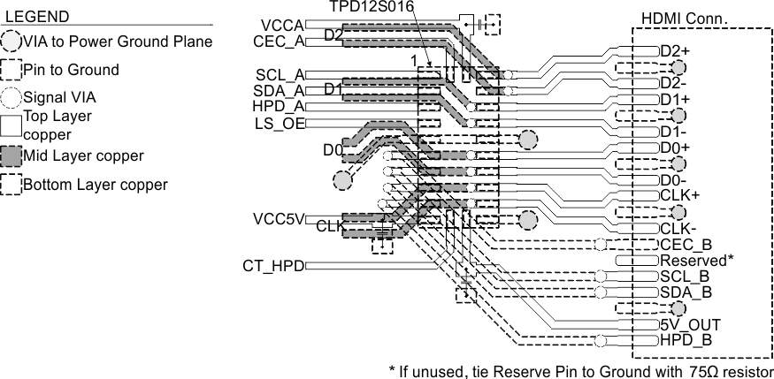
 Figure 19. TPD12S016RKT Layout Example
Routing with TPD12S016RKT requires three layers. Vias are an integral part of layout for such a design. Proper placement of vias can eliminate exposing the system unnecessarily to an ESD event. The example shown above routes the TMDS lines directly from the connector to the protection pins before using vias to an internal layer. This helps promote ESD energy dissipation at the TPD12S016 protection pins. Note that while there is a via between the connector and the DDC/CEC/HPD lines, the traces terminate at the protection pins, leaving no other path for ESD energy to dissipate except at the TPD12S016 protection pins. All ground pins should have a large via near them connecting to as many internal and external ground planes as possible to reduce any impedance between TPD12S016 and ground. Tenting of VIAs near to SMD pads should be done to eliminate any solder-wicking during PCB assembly.
10.2.2 TPD12S016PW
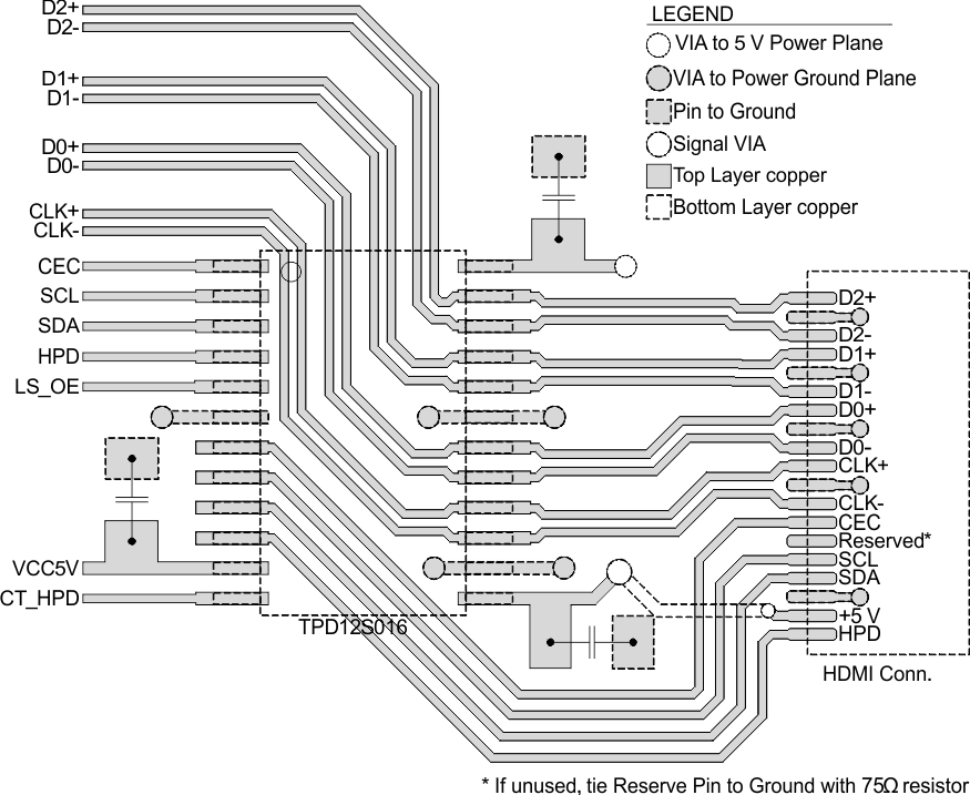
 Figure 20. TPD12S016PW Layout Example
The TPD12S016PW can be routed on a single layer. HDMI connector pin matching has been arranged to allow for a flow through routing style. All ground pins should have a large via near them connecting to as many internal and external ground planes as possible to reduce any impedance between TPD12S016 and ground. Tenting of vias near to SMD pads should be done to eliminate any solder-wicking during PCB assembly.