ZHCS442F September   2011  – November 2016 TPS62080 , TPS62080A , TPS62081 , TPS62082

PRODUCTION DATA.  

  1. 特性
  2. 应用范围
  3. 说明
  4. 修订历史记录
  5. Device Comparison Table
  6. Pin Configuration and Functions
  7. Specifications
    1. 7.1 Absolute Maximum Ratings
    2. 7.2 ESD Ratings
    3. 7.3 Recommended Operating Conditions
    4. 7.4 Thermal Information
    5. 7.5 Electrical Characteristics
    6. 7.6 Typical Characteristics
  8. Detailed Description
    1. 8.1 Overview
    2. 8.2 Functional Block Diagrams
    3. 8.3 Feature Description
      1. 8.3.1 Power Good
      2. 8.3.2 100% Duty Cycle Low Dropout Operation
      3. 8.3.3 Output Discharge
      4. 8.3.4 Soft-Start
      5. 8.3.5 Undervoltage Lockout
      6. 8.3.6 Thermal Shutdown
      7. 8.3.7 Inductor Current Limit
    4. 8.4 Device Functional Modes
      1. 8.4.1 Enabling and Disabling the Device
      2. 8.4.2 Power Save Mode
      3. 8.4.3 Snooze Mode
  9. Application and Implementation
    1. 9.1 Application Information
    2. 9.2 Typical Application
      1. 9.2.1 Design Requirements
      2. 9.2.2 Detailed Design Procedure
        1. 9.2.2.1 Setting the Output Voltage
          1. 9.2.2.1.1 Adjustable Output Voltage Version
        2. 9.2.2.2 Output Filter Design
        3. 9.2.2.3 Inductor Selection
        4. 9.2.2.4 Capacitor Selection
      3. 9.2.3 Application Curves
  10. 10Power Supply Recommendations
  11. 11Layout
    1. 11.1 Layout Guidelines
    2. 11.2 Layout Example
    3. 11.3 Thermal Considerations
  12. 12器件和文档支持
    1. 12.1 器件支持
      1. 12.1.1 Third-Party Products Disclaimer
    2. 12.2 文档支持
      1. 12.2.1 相关文档 
    3. 12.3 相关链接
    4. 12.4 接收文档更新通知
    5. 12.5 社区资源
    6. 12.6 商标
    7. 12.7 静电放电警告
    8. 12.8 Glossary
  13. 13机械、封装和可订购信息

Specifications

Absolute Maximum Ratings

over operating free-air temperature range (unless otherwise noted)(1)
MIN MAX UNIT
Voltage at VIN, PG, VOS(2) –0.3 7 V
Voltage at SW(2)(3) –1 7 V
Voltage at FB(2) –0.3 3.6 V
Voltage at EN, MODE(2) –0.3 VIN + 0.3 V
Sink current at PG 0 0.5 mA
Operating junction temperature, TJ –40 150 °C
Storage temperature, Tstg –65 150 °C
Stresses beyond those listed under Absolute Maximum Ratings may cause permanent damage to the device. These are stress ratings only and functional operation of the device at these or any other conditions beyond those indicated under Recommended Operating Conditions is not implied. Exposure to absolute–maximum–rated conditions for extended periods may affect device reliability.
All voltage values are with respect to network ground terminal.
During operation, device switching.

ESD Ratings

VALUE UNIT
V(ESD) Electrostatic discharge Human body model (HBM), per ANSI/ESDA/JEDEC JS-001(1) ±2000 V
Charged-device model (CDM), per JEDEC specification JESD22-C101(2) ±500
JEDEC document JEP155 states that 500-V HBM allows safe manufacturing with a standard ESD control process.
JEDEC document JEP157 states that 250-V CDM allows safe manufacturing with a standard ESD control process.

Recommended Operating Conditions(1)

MIN NOM MAX UNIT
VIN Input voltage 2.3 6 V
VOUT Output voltage 0.5 4 V
ISNOOZE Load current in Snooze Mode 2 mA
TJ Operating junction temperature –40 125 °C
Refer to the Application and Implementation section for further information.

Thermal Information

THERMAL METRIC(1) TPS6208x UNIT
DSG (WSON)
8 PINS
RθJA Junction-to-ambient thermal resistance 59.7 °C/W
RθJC(top) Junction-to-case (top) thermal resistance 70.1
RθJB Junction-to-board thermal resistance 30.9
ψJT Junction-to-top characterization parameter 1.4
ψJB Junction-to-board characterization parameter 31.5
RθJC(bot) Junction-to-case (bottom) thermal resistance 8.6
For more information about traditional and new thermal metrics, see the Semiconductor and IC Package Thermal Metrics application report.
Electrical Characteristics

Over recommended free-air temperature range, TJ = –40°C to 125°C. Typical values are at TA = 25°C (unless otherwise noted), VIN= 3.6 V, MODE = LOW.
PARAMETER TEST CONDITIONS MIN TYP MAX UNIT
SUPPLY
VIN Input voltage range 2.3 6 V
IQ Quiescent current into VIN IOUT = 0 mA, Device not switching 30 uA
Quiescent current into VIN (SNOOZE MODE) IOUT = 0 mA, Device not switching, MODE=HIGH 6.5 uA
ISD Shutdown current into VIN EN = LOW 7 µA
TA = -40°C to 85°C 1
VUVLO Undervoltage lockout Input voltage falling 1.8 2 V
Undervoltage lockout hysteresis Rising above VUVLO 120 mV
TJSD Thermal shutdown Temperature rising 150 °C
Thermal shutdown hysteresis Temperature falling below TJSD 20 °C
LOGIC INTERFACE (EN MODE)
VIH High level input voltage 2.3 V ≤ VIN ≤ 6 V 1 V
VIL Low level input voltage 2.3 V ≤ VIN ≤ 6 V 0.4 V
ILKG Input leakage current 0.01 0.5 µA
POWER GOOD
VPG Power good threshold VOUT falling referenced to VOUT nominal –15% –10% –5%
Power good hysteresis 5%
VOL Low level voltage Isink = 500 µA 0.3 V
IPG,LKG PG Leakage current VPG = 5.0 V 0.01 0.1 µA
OUTPUT
VOUT Output voltage range
TPS62080, TPS62080A
0.5 4.0 V
Output voltage accuracy
TPS62081
IOUT = 0 mA; VIN ≥ 2.3 V –2.5% 2.5%
Output voltage accuracy
TPS62082
IOUT = 0 mA; VIN ≥ 3.6 V –2.5% 2.5%
Snooze Mode output voltage accuracy MODE = HIGH; VIN ≥ 2.3 V and VIN ≥ VOUT + 1 V –5% 5%
VFB Feedback regulation voltage
TPS62080, TPS62080A
VIN ≥ 2.3 V and VIN ≥ VOUT + 1 V 0.438 0.45 0.462 V
IFB Feedback input bias current
TPS62080, TPS62080A
VFB = 0.45 V 10 100 nA
RDIS Output discharge resistor EN = LOW, VOUT = 1.8 V 1
TPS62080A, EN = LOW, VOUT = 1.2 V 25 40 65 Ω
Line Regulation 0 %/V
Load Regulation TPS62081, TPS62082 –0.25 %/A
RDS(on) High-side FET ON-resistance ISW = 500 mA 95
Low-side FET ON-resistance ISW = 500 mA 70
ILIM High-side FET switch current limit Rising inductor current 1.6 2.8 4 A

Typical Characteristics

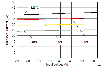
TPS62080 TPS62080A TPS62081 TPS62082 TPS62080_IQ.png Figure 1. Quiescent Current vs Input Voltage in Normal Mode
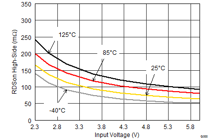
TPS62080 TPS62080A TPS62081 TPS62082 TPS62080_RDSONHS.png Figure 3. High-Side FET RDS(on) vs Input Voltage
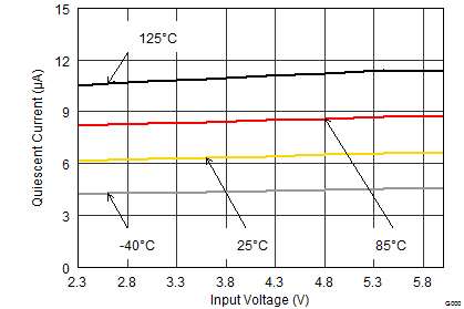
TPS62080 TPS62080A TPS62081 TPS62082 TPS62080_IQ_snooze.png Figure 2. Quiescent Current vs Input Voltage in Snooze Mode
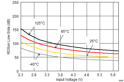
TPS62080 TPS62080A TPS62081 TPS62082 TPS62080_RDSONLS.png Figure 4. Low-Side FET RDS(on) vs Input Voltage