ZHCS484H October 2011 – January 2017 TLV62080 , TLV62084 , TLV62084A
UNLESS OTHERWISE NOTED, this document contains PRODUCTION DATA.
- 1 特性
- 2 应用范围
- 3 说明
- 4 修订历史记录
- 5 Device Comparison Table
- 6 Pin Configurations and Functions
- 7 Specifications
- 8 Detailed Description
- 9 Application and Implementation
- 10Power Supply Recommendations
- 11Layout
- 12器件和文档支持
- 13机械、封装和可订购信息
11 Layout
11.1 Layout Guidelines
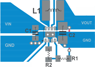
The PCB layout is an important step to maintain the high performance of the TLV62080 and TLV62084x devices.
- Place input and output capacitors, along with the inductor, as close as possible to the IC which keeps the traces short. Routing these traces direct and wide results in low trace resistance and low parasitic inductance.
- Use a common-power GND.
- Properly connect the low side of the input and output capacitors to the power GND to avoid a GND potential shift.
- The sense traces connected to FB and VOS terminals are signal traces. Keep these traces away from SW nodes.
- Use care to avoid noise induction. By a direct routing, parasitic inductance can be kept small.
- Use GND layers for shielding if needed.
11.3 Thermal Considerations
Implementation of integrated circuits in low-profile and fine-pitch surface-mount packages typically requires special attention to power dissipation. Many system-dependent issues such as thermal coupling, airflow, added heat sinks and convection surfaces, and the presence of other heat-generating components affect the power-dissipation limits of a given component.
Three basic approaches for enhancing thermal performance are listed below:
- Improving the power dissipation capability of the PCB design.
- Improving the thermal coupling of the component to the PCB by soldering the Thermal Pad.
- Introducing airflow in the system.
For more details on how to use the thermal parameters, see the Thermal Characteristics application notes SZZA017 and SPRA953.
