ZHCS488K October 2011 – December 2018 AM3351 , AM3352 , AM3354 , AM3356 , AM3357 , AM3358 , AM3359
PRODUCTION DATA.
- 1器件概述
- 2修订历史记录
- 3Device Comparison
- 4Terminal Configuration and Functions
-
5Specifications
- 5.1 Absolute Maximum Ratings
- 5.2 ESD Ratings
- 5.3 Power-On Hours (POH)
- 5.4 Operating Performance Points (OPPs)
- 5.5 Recommended Operating Conditions
- 5.6 Power Consumption Summary
- 5.7 DC Electrical Characteristics
- 5.8 Thermal Resistance Characteristics for ZCE and ZCZ Packages
- 5.9 External Capacitors
- 5.10 Touch Screen Controller and Analog-to-Digital Subsystem Electrical Parameters
-
6Power and Clocking
- 6.1 Power Supplies
- 6.2
Clock Specifications
- 6.2.1 Input Clock Specifications
- 6.2.2 Input Clock Requirements
- 6.2.3 Output Clock Specifications
- 6.2.4 Output Clock Characteristics
-
7Peripheral Information and Timings
- 7.1 Parameter Information
- 7.2 Recommended Clock and Control Signal Transition Behavior
- 7.3 OPP50 Support
- 7.4 Controller Area Network (CAN)
- 7.5 DMTimer
- 7.6
Ethernet Media Access Controller (EMAC) and Switch
- 7.6.1
EMAC and Switch Electrical Data and Timing
- Table 7-7 EMAC and Switch Timing Conditions
- 7.6.1.1 EMAC/Switch MDIO Electrical Data and Timing
- 7.6.1.2
EMAC and Switch MII Electrical Data and Timing
- Table 7-11 Timing Requirements for GMII[x]_RXCLK - MII Mode
- Table 7-12 Timing Requirements for GMII[x]_TXCLK - MII Mode
- Table 7-13 Timing Requirements for GMII[x]_RXD[3:0], GMII[x]_RXDV, and GMII[x]_RXER - MII Mode
- Table 7-14 Switching Characteristics for GMII[x]_TXD[3:0], and GMII[x]_TXEN - MII Mode
- 7.6.1.3 EMAC and Switch RMII Electrical Data and Timing
- 7.6.1.4
EMAC and Switch RGMII Electrical Data and Timing
- Table 7-18 Timing Requirements for RGMII[x]_RCLK - RGMII Mode
- Table 7-19 Timing Requirements for RGMII[x]_RD[3:0], and RGMII[x]_RCTL - RGMII Mode
- Table 7-20 Switching Characteristics for RGMII[x]_TCLK - RGMII Mode
- Table 7-21 Switching Characteristics for RGMII[x]_TD[3:0], and RGMII[x]_TCTL - RGMII Mode
- 7.6.1
EMAC and Switch Electrical Data and Timing
- 7.7
External Memory Interfaces
- 7.7.1 General-Purpose Memory Controller (GPMC)
- 7.7.2
mDDR(LPDDR), DDR2, DDR3, DDR3L Memory Interface
- 7.7.2.1
mDDR (LPDDR) Routing Guidelines
- 7.7.2.1.1 Board Designs
- 7.7.2.1.2 LPDDR Interface
- 7.7.2.1.3 LPDDR CK and ADDR_CTRL Routing
- 7.7.2.2
DDR2 Routing Guidelines
- 7.7.2.2.1 Board Designs
- 7.7.2.2.2
DDR2 Interface
- 7.7.2.2.2.1 DDR2 Interface Schematic
- 7.7.2.2.2.2 Compatible JEDEC DDR2 Devices
- 7.7.2.2.2.3 PCB Stackup
- 7.7.2.2.2.4 Placement
- 7.7.2.2.2.5 DDR2 Keepout Region
- 7.7.2.2.2.6 Bulk Bypass Capacitors
- 7.7.2.2.2.7 High-Speed (HS) Bypass Capacitors
- 7.7.2.2.2.8 Net Classes
- 7.7.2.2.2.9 DDR2 Signal Termination
- 7.7.2.2.2.10 DDR_VREF Routing
- 7.7.2.2.3 DDR2 CK and ADDR_CTRL Routing
- 7.7.2.3
DDR3 and DDR3L Routing Guidelines
- 7.7.2.3.1 Board Designs
- 7.7.2.3.2 DDR3 Device Combinations
- 7.7.2.3.3
DDR3 Interface
- 7.7.2.3.3.1 DDR3 Interface Schematic
- 7.7.2.3.3.2 Compatible JEDEC DDR3 Devices
- 7.7.2.3.3.3 PCB Stackup
- 7.7.2.3.3.4 Placement
- 7.7.2.3.3.5 DDR3 Keepout Region
- 7.7.2.3.3.6 Bulk Bypass Capacitors
- 7.7.2.3.3.7 High-Speed Bypass Capacitors
- 7.7.2.3.3.8 Net Classes
- 7.7.2.3.3.9 DDR3 Signal Termination
- 7.7.2.3.3.10 DDR_VREF Routing
- 7.7.2.3.3.11 VTT
- 7.7.2.3.4 DDR3 CK and ADDR_CTRL Topologies and Routing Definition
- 7.7.2.3.5 Data Topologies and Routing Definition
- 7.7.2.3.6 Routing Specification
- 7.7.2.1
mDDR (LPDDR) Routing Guidelines
- 7.8 I2C
- 7.9 JTAG Electrical Data and Timing
- 7.10 LCD Controller (LCDC)
- 7.11 Multichannel Audio Serial Port (McASP)
- 7.12 Multichannel Serial Port Interface (McSPI)
- 7.13
Multimedia Card (MMC) Interface
- 7.13.1
MMC Electrical Data and Timing
- Table 7-89 MMC Timing Conditions
- Table 7-90 Timing Requirements for MMC[x]_CMD and MMC[x]_DAT[7:0]
- Table 7-91 Switching Characteristics for MMC[x]_CLK
- Table 7-92 Switching Characteristics for MMC[x]_CMD and MMC[x]_DAT[7:0]—Standard Mode
- Table 7-93 Switching Characteristics for MMC[x]_CMD and MMC[x]_DAT[7:0]—High-Speed Mode
- 7.13.1
MMC Electrical Data and Timing
- 7.14
Programmable Real-Time Unit Subsystem and Industrial Communication Subsystem (PRU-ICSS)
- 7.14.1 Programmable Real-Time Unit (PRU-ICSS PRU)
- 7.14.2
PRU-ICSS EtherCAT (PRU-ICSS ECAT)
- Table 7-100 PRU-ICSS ECAT Timing Conditions
- 7.14.2.1
PRU-ICSS ECAT Electrical Data and Timing
- Table 7-101 PRU-ICSS ECAT Timing Requirements – Input Validated With LATCH_IN
- Table 7-102 PRU-ICSS ECAT Timing Requirements – Input Validated With SYNCx
- Table 7-103 PRU-ICSS ECAT Timing Requirements – Input Validated With Start of Frame (SOF)
- Table 7-104 PRU-ICSS ECAT Timing Requirements - LATCHx_IN
- Table 7-105 PRU-ICSS ECAT Switching Requirements - Digital I/Os
- 7.14.3 PRU-ICSS MII_RT and Switch
- 7.14.4 PRU-ICSS Universal Asynchronous Receiver Transmitter (PRU-ICSS UART)
- 7.15 Universal Asynchronous Receiver Transmitter (UART)
- 8Device and Documentation Support
- 9Mechanical, Packaging, and Orderable Information
Table 7-28 GPMC and NOR Flash Switching Characteristics—Asynchronous Mode
| NO. | PARAMETER | OPP100 | OPP50 | UNIT | ||||
|---|---|---|---|---|---|---|---|---|
| MIN | MAX | MIN | MAX | |||||
| FA0 | tw(be[x]nV) | Pulse duration, output lower-byte enable and command latch enable gpmc_be0n_cle, output upper-byte enable gpmc_be1n valid time | Read | N(12) | N(12) | ns | ||
| Write | N(12) | N(12) | ||||||
| FA1 | tw(csnV) | Pulse duration, output chip select gpmc_csn[x](13) low | Read | A(1) | A(1) | ns | ||
| Write | A(1) | A(1) | ||||||
| FA3 | td(csnV-advnIV) | Delay time, output chip select gpmc_csn[x](13) valid to output address valid and address latch enable gpmc_advn_ale invalid | Read | B(2) – 0.2 | B(2) + 2.0 | B(2) – 5 | B(2) + 5 | ns |
| Write | B(2) – 0.2 | B(2) + 2.0 | B(2) – 5 | B(2) + 5 | ||||
| FA4 | td(csnV-oenIV) | Delay time, output chip select gpmc_csn[x](13) valid to output enable gpmc_oen invalid (Single read) | C(3) – 0.2 | C(3) + 2.0 | C(3) – 5 | C(3) + 5 | ns | |
| FA9 | td(aV-csnV) | Delay time, output address gpmc_a[27:1] valid to output chip select gpmc_csn[x](13) valid | J(9) – 0.2 | J(9) + 2.0 | J(9) – 5 | J(9) + 5 | ns | |
| FA10 | td(be[x]nV-csnV) | Delay time, output lower-byte enable and command latch enable gpmc_be0n_cle, output upper-byte enable gpmc_be1n valid to output chip select gpmc_csn[x](13) valid | J(9) – 0.2 | J(9) + 2.0 | J(9) – 5 | J(9) + 5 | ns | |
| FA12 | td(csnV-advnV) | Delay time, output chip select gpmc_csn[x](13) valid to output address valid and address latch enable gpmc_advn_ale valid | K(10) – 0.2 | K(10) + 2.0 | K(10) – 5 | K(10) + 5 | ns | |
| FA13 | td(csnV-oenV) | Delay time, output chip select gpmc_csn[x](13) valid to output enable gpmc_oen valid | L(11) – 0.2 | L(11) + 2.0 | L (11) – 5 | L(11) + 5 | ns | |
| FA16 | tw(aIV) | Pulse durationm output address gpmc_a[26:1] invalid between 2 successive read and write accesses | G(7) | G(7) | ns | |||
| FA18 | td(csnV-oenIV) | Delay time, output chip select gpmc_csn[x](13) valid to output enable gpmc_oen invalid (Burst read) | I(8) – 0.2 | I(8) + 2.0 | I(8) – 5 | I(8) + 5 | ns | |
| FA20 | tw(aV) | Pulse duration, output address gpmc_a[27:1] valid - 2nd, 3rd, and 4th accesses | D(4) | D(4) | ns | |||
| FA25 | td(csnV-wenV) | Delay time, output chip select gpmc_csn[x](13) valid to output write enable gpmc_wen valid | E(5) – 0.2 | E(5) + 2.0 | E(5) – 5 | E(5) + 5 | ns | |
| FA27 | td(csnV-wenIV) | Delay time, output chip select gpmc_csn[x](13) valid to output write enable gpmc_wen invalid | F(6) – 0.2 | F(6) + 2.0 | F(6) – 5 | F(6) + 5 | ns | |
| FA28 | td(wenV-dV) | Delay time, output write enable gpmc_ wen valid to output data gpmc_ad[15:0] valid | 2.0 | 5 | ns | |||
| FA29 | td(dV-csnV) | Delay time, output data gpmc_ad[15:0] valid to output chip select gpmc_csn[x](13) valid | J(9) – 0.2 | J(9) + 2.0 | J(9) – 5 | J(9) + 5 | ns | |
| FA37 | td(oenV-aIV) | Delay time, output enable gpmc_oen valid to output address gpmc_ad[15:0] phase end | 2.0 | 5 | ns | |||
- For single read: A = (CSRdOffTime – CSOnTime) × (TimeParaGranularity + 1) × GPMC_FCLK(14)
For single write: A = (CSWrOffTime – CSOnTime) × (TimeParaGranularity + 1) × GPMC_FCLK(14)
For burst read: A = (CSRdOffTime – CSOnTime + (n – 1) × PageBurstAccessTime) × (TimeParaGranularity + 1) × GPMC_FCLK(14)
For burst write: A = (CSWrOffTime – CSOnTime + (n – 1) × PageBurstAccessTime) × (TimeParaGranularity + 1) × GPMC_FCLK(14)
with n being the page burst access number - For reading: B = ((ADVRdOffTime – CSOnTime) × (TimeParaGranularity + 1) + 0.5 × (ADVExtraDelay – CSExtraDelay)) × GPMC_FCLK(14)
For writing: B = ((ADVWrOffTime – CSOnTime) × (TimeParaGranularity + 1) + 0.5 × (ADVExtraDelay – CSExtraDelay)) × GPMC_FCLK(14) - C = ((OEOffTime – CSOnTime) × (TimeParaGranularity + 1) + 0.5 × (OEExtraDelay – CSExtraDelay)) × GPMC_FCLK(14)
- D = PageBurstAccessTime × (TimeParaGranularity + 1) × GPMC_FCLK(14)
- E = ((WEOnTime – CSOnTime) × (TimeParaGranularity + 1) + 0.5 × (WEExtraDelay – CSExtraDelay)) × GPMC_FCLK(14)
- F = ((WEOffTime – CSOnTime) × (TimeParaGranularity + 1) + 0.5 × (WEExtraDelay – CSExtraDelay)) × GPMC_FCLK(14)
- G = Cycle2CycleDelay × GPMC_FCLK(14)
- I = ((OEOffTime + (n – 1) × PageBurstAccessTime – CSOnTime) × (TimeParaGranularity + 1) + 0.5 × (OEExtraDelay – CSExtraDelay)) × GPMC_FCLK(14)
- J = (CSOnTime × (TimeParaGranularity + 1) + 0.5 × CSExtraDelay) × GPMC_FCLK(14)
- K = ((ADVOnTime – CSOnTime) × (TimeParaGranularity + 1) + 0.5 × (ADVExtraDelay – CSExtraDelay)) × GPMC_FCLK(14)
- L = ((OEOnTime – CSOnTime) × (TimeParaGranularity + 1) + 0.5 × (OEExtraDelay – CSExtraDelay)) × GPMC_FCLK(14)
- For single read: N = RdCycleTime × (TimeParaGranularity + 1) × GPMC_FCLK(14)
For single write: N = WrCycleTime × (TimeParaGranularity + 1) × GPMC_FCLK(14)
For burst read: N = (RdCycleTime + (n – 1) × PageBurstAccessTime) × (TimeParaGranularity + 1) × GPMC_FCLK(14)
For burst write: N = (WrCycleTime + (n – 1) × PageBurstAccessTime) × (TimeParaGranularity + 1) × GPMC_FCLK(14) - In gpmc_csn[x], x is equal to 0, 1, 2, 3, 4, or 5.
- GPMC_FCLK is general-purpose memory controller internal functional clock period in ns.
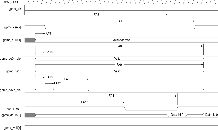
A. In gpmc_csn[x], x is equal to 0, 1, 2, 3, 4, or 5. In gpmc_wait[x], x is equal to 0 or 1.
B. FA5 parameter illustrates amount of time required to internally sample input data. It is expressed in number of GPMC functional clock cycles. From start of read cycle and after FA5 functional clock cycles, input data will be internally sampled by active functional clock edge. FA5 value must be stored inside AccessTime register bits field.
C. GPMC_FCLK is an internal clock (GPMC functional clock) not provided externally.
Figure 7-22 GPMC and NOR Flash—Asynchronous Read—Single WordABC 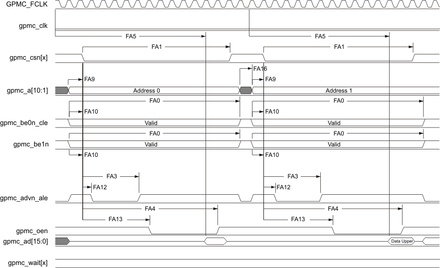
A. In gpmc_csn[x], x is equal to 0, 1, 2, 3, 4, or 5. In gpmc_wait[x], x is equal to 0 or 1.
B. FA5 parameter illustrates amount of time required to internally sample input data. It is expressed in number of GPMC functional clock cycles. From start of read cycle and after FA5 functional clock cycles, input data will be internally sampled by active functional clock edge. FA5 value must be stored inside AccessTime register bits field.
C. GPMC_FCLK is an internal clock (GPMC functional clock) not provided externally.
Figure 7-23 GPMC and NOR Flash—Asynchronous Read—32-BitABC 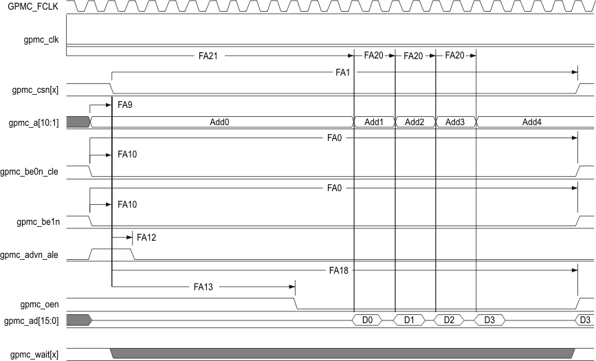
A. In gpmc_csn[x], x is equal to 0, 1, 2, 3, 4, or 5. In gpmc_wait[x], x is equal to 0 or 1.
B. FA21 parameter illustrates amount of time required to internally sample first input page data. It is expressed in number of GPMC functional clock cycles. From start of read cycle and after FA21 functional clock cycles, first input page data will be internally sampled by active functional clock edge. FA21 calculation must be stored inside AccessTime register bits field.
C. FA20 parameter illustrates amount of time required to internally sample successive input page data. It is expressed in number of GPMC functional clock cycles. After each access to input page data, next input page data will be internally sampled by active functional clock edge after FA20 functional clock cycles. FA20 is also the duration of address phases for successive input page data (excluding first input page data). FA20 value must be stored in PageBurstAccessTime register bits field.
D. GPMC_FCLK is an internal clock (GPMC functional clock) not provided externally.
Figure 7-24 GPMC and NOR Flash—Asynchronous Read—Page Mode 4x16-BitABCD 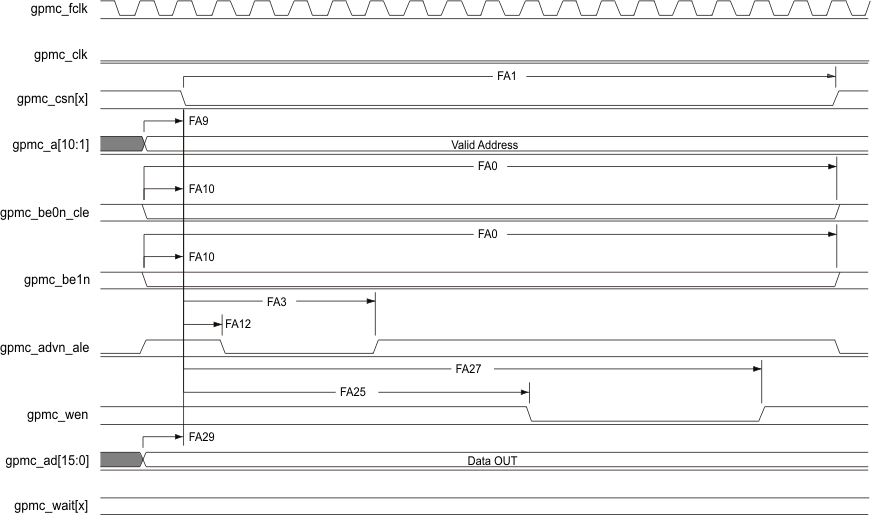
A. In gpmc_csn[x], x is equal to 0, 1, 2, 3, 4, or 5. In gpmc_wait[x], x is equal to 0 or 1.
Figure 7-25 GPMC and NOR Flash—Asynchronous Write—Single WordA 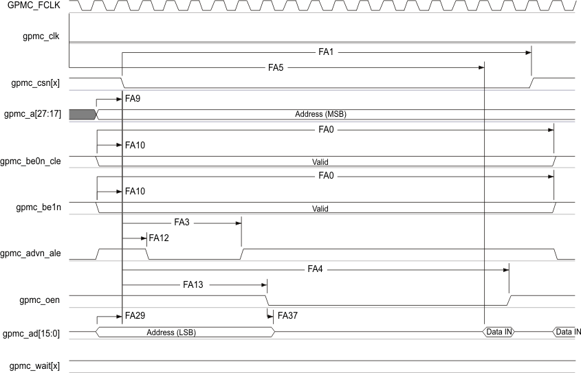
A. In gpmc_csn[x], x is equal to 0, 1, 2, 3, 4, or 5. In gpmc_wait[x], x is equal to 0 or 1.
B. FA5 parameter illustrates amount of time required to internally sample input data. It is expressed in number of GPMC functional clock cycles. From start of read cycle and after FA5 functional clock cycles, input data will be internally sampled by active functional clock edge. FA5 value must be stored inside AccessTime register bits field.
C. GPMC_FCLK is an internal clock (GPMC functional clock) not provided externally.
Figure 7-26 GPMC and Multiplexed NOR Flash—Asynchronous Read—Single WordABC 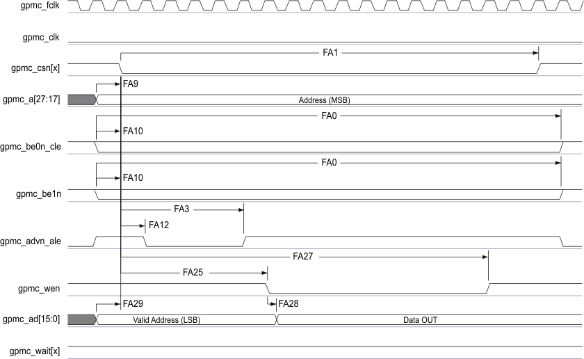
A. In gpmc_csn[x], x is equal to 0, 1, 2, 3, 4, or 5. In gpmc_wait[x], x is equal to 0 or 1.
Figure 7-27 GPMC and Multiplexed NOR Flash—Asynchronous Write—Single WordA