ZHCS609A December 2011 – November 2016 TPS53316
PRODUCTION DATA.
- 1 特性
- 2 应用
- 3 说明
- 4 修订历史记录
- 5 Pin Configuration and Functions
- 6 Specifications
- 7 Detailed Description
- 8 Application and Implementation
- 9 Power Supply Recommendations
- 10Layout
- 11器件和文档支持
- 12机械、封装和可订购信息
7 Detailed Description
7.1 Overview
The TPS53316 is a high-efficiency switching regulator with two integrated N-channel MOSFETs and is capable of delivering up to 5 A of load current. The TPS53316 provides output voltage from 0.6 V up to 0.8 × VIN from
2.9-V to 6-V wide input voltage range.
This device employs 3 operation modes to fit into various application requirements. The skip mode operation provides reduced power loss and increases the efficiency at light load. The unique, patented PWM modulator enables smooth light load to heavy load transition while maintaining fast load transient.
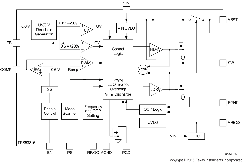
7.2 Functional Block Diagram

7.3 Feature Description
7.3.1 Overcurrent and Frequency Setting
The overcurrent and frequency setting are determined by RF/OC pin connection as shown in Table 1. At start-up, the RF/OC pin sources 10-µA current and then sense the voltage on this pin to determine the switching frequency and OCP threshold.
Table 1. Overcurrent and Frequency Setting
| RF/OC PIN CONNECTION | FREQUENCY (kHz) | OVERCURRENT THRESHOLD (A) |
|---|---|---|
| GND | 1100 | 6.5 |
| 24.3 kΩ to GND | 750 | 4.5 |
| 57.6 kΩ to GND | 750 | 6.5 |
| 105 kΩ to GND | 2000 | 4.5 |
| 174 kΩ to GND | 2000 | 6.5 |
| Floating or pulled to VREG3 | 1100 | 4.5 |
7.3.2 Soft-Start Operation
The soft-start operation reduces the inrush current during the start-up time. A slow rising reference is generated by the soft-start circuitry and send to the input of the error amplifier. When the soft-start ramp voltage is less than 600 mV, the error amplifier uses this ramp voltage as the reference. When the ramp voltage reaches 600 mV, the error amplifier switch to a fixed 600-mV reference. The typical soft-start time is 400 µs for 1 × soft-start time setting and 1.6 ms for 4 times the soft-start time setting.
7.3.3 Power Good
The TPS53316 monitors the voltage on the FB pin. If the FB voltage is within 117% and 83% of the reference voltage, the power good signal remains high. If FB voltage is out of this window, power good pin is pulled low by the internal open-drain output.
During start-up operation, the input voltage must be higher than 1 V to have valid power good logic, and the power good signal has 300 µs (1.2 ms with 4 times setting) delay after FB falling into the power good window. There is also 10-µs delay during shutdown after FB falling out of the power good window.
7.3.4 UVLO Function
The TPS53316 provides UVLO protection for input voltage. If the input voltage is higher than UVLO threshold voltage, the device starts up. When the voltage becomes lower than the threshold voltage minus the hysteresis, the device shuts off. The typical UVLO rising threshold is 2.8 V and the hysteresis is 130 mV.
A similar UVLO function is provided to the VREG3 pin. The typical UVLO rising threshold is 2.8 V and the hysteresis is 75 mV for VREG3.
7.3.5 Overcurrent Protection
The TPS53316 continuously monitors the current flowing through high-side and low-side MOSFETs. If the current through the high-side FET exceeds 6.8 A (or 4.5 A with 4.5-A setting), the high-side FET turns off and the low-side FET turns on. An OC counter starts to increment to count the occurrence of the overcurrent events. The converter shuts down immediately when the OC counter reaches 4. The OC counter resets if the detected current is less 6.8 A after an OC event.
Another set of overcurrent circuitry monitors the current through low-side FET. If the current through the low-side FET exceeds 7.5 A (or 5.1 A with 4.5-A setting), the overcurrent protection is engaged and turns off both high-side and low-side FETs immediately. The device is fully protected against overcurrent during both on-time and off-time.
After an OCP event, the device attempts to restart after a hiccup delay (14.5 ms typical). If the OC condition clears before restart, the device starts up normally. Otherwise the hiccup process repeats.
7.3.6 Overvoltage Protection
The TPS53316 monitors the voltage divided feedback voltage to detect the overvoltage and undervoltage conditions. When the feedback voltage is greater than 117% of the reference, the high-side MOSFET turns off and the low-side MOSFET turns on. Then the output voltage drops and reaches the undervoltage threshold. At that point the low-side MOSFET turns off and the device enters high-impedance state.
7.3.7 Undervoltage Protection
When the feedback voltage is lower than 83% of the reference voltage, the undervoltage protection counter starts. If the feedback voltage remains lower than the undervoltage threshold voltage after 10 µs, the device turns off both high-side and low-side MOSFETs and enters high-impedance state. After a hiccup delay (14.5 ms typical), the device attempts to restart. If the UV condition clears before restart, the device starts up normally. Otherwise the hiccup process repeats.
7.3.8 Overtemperature Protection
The TPS53316 continuously monitors the die temperature. If the die temperature exceeds the threshold value (140°C typical), the device shuts off. When the device is cooled to 40°C below the overtemperature threshold, it restarts and returns to normal operation.
7.3.9 Output Discharge
When the EN pin is low, the TPS53316 discharges the output capacitors through an internal MOSFET switch between SW and GND while the high-side and low-side MOSFETs remain OFF. The typical discharge switch-ON resistance is 60 Ω. This function is disabled when the input voltage is less than 1 V.
7.4 Device Functional Modes
7.4.1 Operation Mode
The TPS53316 has 3 operation modes determined by PS connection as listed in Table 2. Each mode has two soft-start and power good delay options (1 time and 4 times). At start-up, the PS pin sources 10 µA of current and then sense the voltage on this pin to determine the operation mode and soft-start time.
Table 2. Operation Mode Selection
| PS PIN CONNECTION | OPERATION MODE | AUTO-SKIP AT LIGHT LOAD | SOFT-START TIME |
|---|---|---|---|
| GND | FCCM | No | 4 times |
| 24.3 kΩ to GND | HEF Mode | Yes | 4 times |
| 57.6 kΩ to GND | HEF Mode | Yes | 1 times |
| 105 kΩ to GND | DE Mode | Yes | 1 time |
| 174 kΩ to GND | DE Mode | Yes | 4 times |
| Floating or pulled to VREG3 | FCCM | No | 1 time |
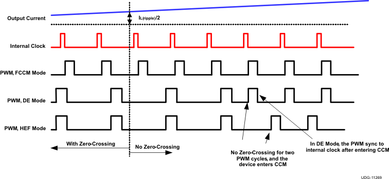
In forced continuous conduction mode (FCCM), the high-side FET is ON during the on-time and low-side FET is ON during the off-time. The switching is synchronized to the internal clock thus the switching frequency is fixed.
In diode emulation mode (DE), the high-side FET is ON during the on-time and low-side FET is ON during the off-time until the inductor current reaches zero. An internal zero-crossing comparator detects the zero crossing of inductor current from positive to negative. When the inductor current reaches zero, the comparator sends a signal to the logic control and turns off the low-side FET.
When the load is increased, the inductor current is always positive and the zero-crossing comparator does not send a zero-crossing signal. The converter enters into continuous conduction mode (CCM) when no zero-crossing is detected for two consecutive PWM pulses. The switching is synchronized to the internal clock and the switching frequency is fixed.
In high-efficiency mode (HEF), the converter does not synchronize to internal clock during CCM. Instead, the PWM modulator determines the switching frequency. The operation in discontinuous conduction mode (DCM) is the same as DE mode.
In both DE and HEF modes, the device operates under CCM with fixed SW frequency if the load current is higher than half of the inductor ripple current. When the load current is decreased and seven consecutive zero-crossing events are detected, the device enters DCM and light load control is enabled. The on-pulse in DCM is designed to be 25% higher than CCM to provide hysteresis to avoid chattering between CCM and DCM.
The PS pins also set the soft-start time and power good start-up delay of the device. The nominal sort-start time is 400 µs from the time VOUT = 0 V to when VOUT = 100%, and the nominal power good delay is 300 µs from the time VOUT = 100% to when power good is asserted. When the PS pin is connected to GND directly or with a resistor with a value of 24.3 kΩ or 174 kΩ, the soft-start time and power good delay is 4 times the nominal (1.6 ms for soft-start time and 1.2 ms for power good delay).
7.4.2 Light Load Operation
In skip modes (DE and HEF) when the load current is less than half of inductor ripple current, the inductor current reaches zero by the end of off-time. The light load control scheme then turns off the low-side MOSFET when inductor current reaches zero. Because there is no negative inductor current, the energy delivered to the load per switching cycle is increased compared to the normal PWM mode operation. The controller then reduces the switching frequency to maintain the output voltage regulation. The switching loss is reduced and thus efficiency is improved.
In both DE and HEF mode, when the load current decreases, the switching frequency also decreases continuously in discontinuous conduction mode (DCM). When the load current is 0 A, the minimum switching frequency is reached. It is also required that the difference between VVBST and VSW to be higher than 2.4 V to ensure the supply for high-side gate driver.
 Figure 37. TPS53316 Operation Modes in Light and Heavy Load Conditions
7.4.3 Forced Continuous Conduction Mode
When the PS pin is grounded or greater than 2.2 V, the TPS53316 is operating in continuous conduction mode in both light and heavy load condition. In this mode, the switching frequency remains constant over the entire load range which is suitable for applications requiring tight control of switching frequency at a cost of lower efficiency at light load.