ZHCS688I November 2011 – March 2018 TPS65217
PRODUCTION DATA.
- 1 特性
- 2 应用
- 3 说明
- 4 修订历史记录
- 5 Device Comparison Table
- 6 Pin Configuration and Functions
- 7 Specifications
-
8 Detailed Description
- 8.1 Overview
- 8.2 Functional Block Diagram
- 8.3
Feature Description
- 8.3.1 Wake-Up and Power-Up Sequencing
- 8.3.2 Power Good
- 8.3.3 Push-Button Monitor (PB_IN)
- 8.3.4 nWAKEUP Pin (nWAKEUP)
- 8.3.5 Power Enable Pin (PWR_EN)
- 8.3.6 Reset Pin (nRESET)
- 8.3.7 Interrupt Pin (nINT)
- 8.3.8 Analog Multiplexer
- 8.3.9 Battery Charger and Power Path
- 8.3.10 Battery Charging
- 8.3.11 Precharge
- 8.3.12 Charge Termination
- 8.3.13 Battery Detection and Recharge
- 8.3.14 Safety Timer
- 8.3.15 Battery-Pack Temperature Monitoring
- 8.3.16 DC/DC Converters
- 8.3.17 Standby LDO Regulators (LDO1, LDO2)
- 8.3.18 Load Switches or LDO Regulators (LS1 or LDO3, LS2 or LDO4)
- 8.3.19 White LED Driver
- 8.4 Device Functional Modes
- 8.5 Programming
- 8.6
Register Maps
- 8.6.1 Register Address Map
- 8.6.2 Chip ID Register (CHIPID) (Address = 0x00) [reset = X]
- 8.6.3 Power Path Control Register (PPATH) (Address = 0x01) [reset = 0x3D]
- 8.6.4 Interrupt Register (INT) (Address = 0x02) [reset = 0x80]
- 8.6.5 Charger Configuration Register 0 (CHGCONFIG0) (Address = 0x03) [reset = 0x00]
- 8.6.6 Charger Configuration Register 1 (CHGCONFIG1) (Address = 0x04) [reset = 0xB1]
- 8.6.7 Charger Configuration Register 2 (CHGCONFIG2) (Address = 0x05) [reset = 0x80]
- 8.6.8 Charger Configuration Register 3 (CHGCONFIG3) (Address = 0x06) [reset = 0xB2]
- 8.6.9 WLED Control Register 1 (WLEDCTRL1) (Address = 0x07) [reset = 0xB1]
- 8.6.10 WLED Control Register 2 (WLEDCTRL2) (Address = 0x08) [reset = 0x00]
- 8.6.11 MUX Control Register (MUXCTRL) (Address = 0x09) [reset = 0x00]
- 8.6.12 Status Register (STATUS) (Address = 0x0A) [reset = 0x00]
- 8.6.13 Password Register (PASSWORD) (Address = 0x0B) [reset = 0x00]
- 8.6.14 Power Good Register (PGOOD) (Address = 0x0C) [reset = 0x00]
- 8.6.15 Power-Good Control Register (DEFPG) (Address = 0x0D) [reset = 0x0C]
- 8.6.16 DCDC1 Control Register (DEFDCDC1) (Address = 0x0E) [reset = X]
- 8.6.17 DCDC2 Control Register (DEFDCDC2) (Address = 0x0F) [reset = X]
- 8.6.18 DCDC3 Control Register (DEFDCDC3) (Address = 0x10) [reset = 0x08]
- 8.6.19 Slew-Rate Control Register (DEFSLEW) (Address = 0x11) [reset = 0x06]
- 8.6.20 LDO1 Control Register (DEFLDO1) (Address = 0x12) [reset = 0x09]
- 8.6.21 LDO2 Control Register (DEFLDO2) (Address = 0x13) [reset = 0x38]
- 8.6.22 Load Switch1 or LDO3 Control Register (DEFLS1) (Address = 0x14) [reset = X]
- 8.6.23 Load Switch2 or LDO4 Control Register (DEFLS2) (Address = 0x15) [reset = X]
- 8.6.24 Enable Register (ENABLE) (Address = 0x16) [reset = 0x00]
- 8.6.25 UVLO Control Register (DEFUVLO) (Address = 0x18) [reset = 0x03]
- 8.6.26 Sequencer Register 1 (SEQ1) (Address = 0x19) [reset = X]
- 8.6.27 Sequencer Register 2 (SEQ2) (Address = 0x1A) [reset = X]
- 8.6.28 Sequencer Register 3 (SEQ3) (Address = 0x1B) [reset = X]
- 8.6.29 Sequencer Register 4 (SEQ4) (Address = 0x1C) [reset = 0x40]
- 8.6.30 Sequencer Register 5 (SEQ5) (Address = 0x1D) [reset = X]
- 8.6.31 Sequencer Register 6 (SEQ6) (Address = 0x1E) [reset = 0x00]
- 9 Application and Implementation
- 10Power Supply Recommendations
- 11Layout
- 12器件和文档支持
- 13机械、封装和可订购信息
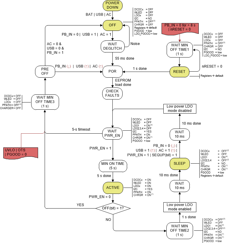
8.4 Device Functional Modes

1. Only if USB or AC supply is present
2. Rails are powered-down as controlled by the sequencer in default EEPROM settings
3. Battery voltage always supplies the system (from BAT pin to SYS pin)
4. LDO1 is assigned to STROBE15 in default EEPROM settings and this special strobe is not controlled by the sequencer. LDO1 can only source 1 mA in the SLEEP state
5. The 9-MHz oscillator is enabled only when WLED or DCDC or PPATH or CHARGER is enabled.
6. The charger, auto-discharge, PPATH, and 9-MHz oscillator are ON in the SLEEP state if AC or USB is present and the charger is enabled and not fully charged.
7. Any USB = 1(↑) or AC = 1 (↑) event in the WAIT MIN OFF TIME2 state makes the device go from the SLEEP state when the timer expires. Any USB = 1(↑) or AC = 1 (↑) event in the WAIT MIN OFF TIME3 state makes the device go from the PRE-OFF state when the timer expires.
8. All user registers are reset to default values each time the device goes to the SLEEP state.
9. UVLO and OTS are monitored in all the states except the OFF, POR, and WAIT DEGLITCH states.
Figure 24. Global State Diagram