ZHCS759E February 2012 – September 2016 TLV62150 , TLV62150A
PRODUCTION DATA.
- 1 特性
- 2 应用
- 3 说明
- 4 修订历史记录
- 5 Device Comparison Table
- 6 Pin Configuration and Functions
- 7 Specifications
- 8 Detailed Description
- 9 Application and Implementation
- 10Power Supply Recommendations
- 11Layout
- 12器件和文档支持
- 13机械、封装和可订购信息
9 Application and Implementation
spacing
NOTE
Information in the following applications sections is not part of the TI component specification, and TI does not warrant its accuracy or completeness. TI’s customers are responsible for determining suitability of components for their purposes. Customers should validate and test their design implementation to confirm system functionality.
spacing
9.1 Application Information
The TLV62150 is a switched-mode step-down converter, able to convert a 4-V to 17-V input voltage into a 0.9-V to 5-V output voltage, providing up to 1 A. It needs a minimum amount of external components. Apart from the LC output filter and the input capacitor, the TLV62150 (TLV62150A) needs an additional resistive divider to set the output voltage level.
9.2 Typical Application
Figure 5 shows an application for Point-of-Load Power Supply Using TLV62150.
spacing
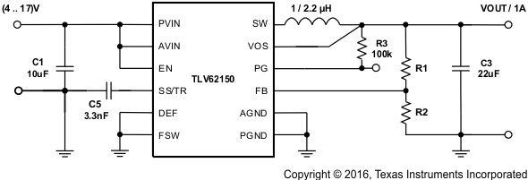 Figure 5. 1-A Step-Down Converter
spacing
9.2.1 Design Requirements
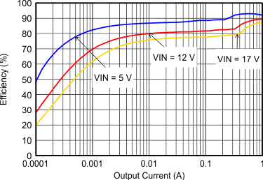
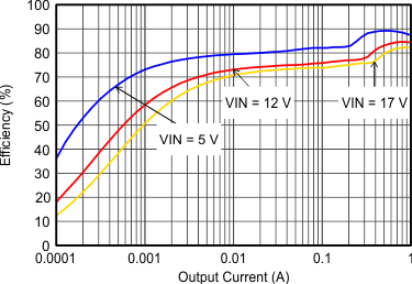
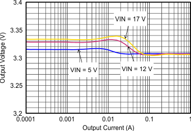
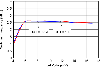
The following design guideline provides a component selection to operate the device within the recommended operating conditions. Using the FSW pin, the design can be optimized for highest efficiency or smallest solution size and lowest output voltage ripple. For highest efficiency set FSW=High and the device operates at the lower switching frequency. For smallest solution size and lowest output voltage ripple set FSW=Low and the device operates with higher switching frequency. The typical values for all measurements are VIN = 12 V, VOUT = 3.3 V and T = 25°C, using the external components of Table 3.
9.2.2 Detailed Design Procedure
The component selection used for measurements is given as follows:
Table 3. List of Components
| REFERENCE | DESCRIPTION | MANUFACTURER(1) |
|---|---|---|
| IC | 17-V, 1-A Step-Down Converter, VQFN | TLV62150RGT, Texas Instruments |
| L1 | 2.2 µH, 0.165 × 0.165 in | XFL4020-222MEB, Coilcraft |
| C1 | 10 µF, 25 V, Ceramic | Standard |
| C3 | 22 µF, 6.3 V, Ceramic | Standard |
| C5 | 3300 pF, 25 V, Ceramic | |
| R1 | depending on Vout | |
| R2 | depending on Vout | |
| R3 | 100 kΩ, Chip, 0603, 1/16 W, 1% | Standard |
9.2.2.1 Programming the Output Voltage
The output voltage of the TLV62150 (TLV62150A) is adjustable. It can be programmed for output voltages from 0.9 V to 5 V by using a resistive divider from VOUT to AGND. The voltage at the FB pin is regulated to 800 mV. The value of the output voltage is set by the selection of the resistive divider from Equation 6. It is recommended to choose resistor values which allow a current of at least 2 µA, meaning the value of R2 should not exceed 400 kΩ. Lower resistor values are recommended for highest accuracy and most robust design.

In case the FB pin gets opened, the device clamps the output voltage at the VOS pin internally to about 7.4 V.
9.2.2.2 External Component Selection
The external components have to fulfill the needs of the application, but also the stability criteria of the devices control loop. The TLV62150 is optimized to work within a range of external components. The LC output filter's inductance and capacitance have to be considered in conjunction, creating a double pole, responsible for the corner frequency of the converter (see Output Filter and Loop Stability section). Table 4 can be used to simplify the output filter component selection. Checked cells represent combinations that are proven for stability by simulation and lab test. Further combinations should be checked for each individual application. See SLVA463 for details.
Table 4. L-C Output Filter Combinations(1)
| 4.7 µF | 10 µF | 22 µF | 47 µF | 100 µF | 200 µF | 400 µF | |
|---|---|---|---|---|---|---|---|
| 0.47 µH | |||||||
| 1 µH | √ | √ | √ | √ | |||
| 2.2 µH | √ | √(2) | √ | √ | √ | ||
| 3.3 µH | √ | √ | √ | √ | |||
| 4.7 µH |
spacing
The TLV62150 can be run with an inductor as low as 1 µH or 2.2 µH. FSW should be set Low in this case. However, for applications running with the low frequency setting (FSW=High) or with low input voltages, 3.3 µH is recommended.
9.2.2.2.1 Inductor Selection
The inductor selection is affected by several effects like inductor ripple current, output ripple voltage, PWM-to-PSM transition point and efficiency. In addition, the inductor selected has to be rated for appropriate saturation current and DC resistance (DCR). Equation 7 and Equation 8 calculate the maximum inductor current under static load conditions.
spacing

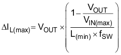
where
- IL(max) is the maximum inductor current.
- ΔIL is the Peak to Peak Inductor Ripple Current.
- L(min) is the minimum effective inductor value.
- fSW is the actual PWM Switching Frequency.
spacing
Calculating the maximum inductor current using the actual operating conditions gives the minimum saturation current of the inductor needed. A margin of about 20% is recommended to add. A larger inductor value is also useful to get lower ripple current, but increases the transient response time and size as well. The following inductors have been used with the TLV62150 and are recommended for use:
Table 5. List of Inductors
| Type | Inductance [µH] | Saturation Current [A](1) | Dimensions [L x B x H] mm | MANUFACTURER(2) |
|---|---|---|---|---|
| XFL4020-222ME_ | 2.2 µH, ±20% | 3.5 | 4 × 4 × 2.1 | Coilcraft |
| XFL3012-222MEC | 2.2 µH, ±20% | 1.6 | 3 × 3 × 1.2 | Coilcraft |
| XFL3012-332MEC | 3.3 µH, ±20% | 1.4 | 3 × 3 × 1.2 | Coilcraft |
| VLS252012T-2R2M1R3 | 2.2 µH, ±20% | 1.3 | 2.5 × 2 × 1.2 | TDK |
| LPS3015-332 | 3.3 µH, ±20% | 1.4 | 3 × 3 × 1.4 | Coilcraft |
| 744025003 | 3.3 µH, ±20% | 1.5 | 2.8 × 2.8 × 2.8 | Wuerth |
| PSI25201B-2R2MS | 2.2 µH, ±20% | 1.3 | 2 × 2.5 × 1.2 | Cyntec |
| NR3015T-2R2M | 2.2 µH, ±20% | 1.5 | 3 × 3 × 1.5 | Taiyo Yuden |
spacing
The inductor value also determines the load current at which Power Save Mode is entered:

Using Equation 8, this current level can be adjusted by changing the inductor value.
9.2.2.2.2 Capacitor Selection
9.2.2.2.2.1 Output Capacitor
The recommended value for the output capacitor is 22 µF. The architecture of the TLV62150 allows the use of tiny ceramic output capacitors which have low equivalent series resistance (ESR). These capacitors provide low output voltage ripple and are recommended. To keep its low resistance up to high frequencies and to get narrow capacitance variation with temperature, it's recommended to use X7R or X5R dielectric. Using a higher value can have some advantages like smaller voltage ripple and a tighter DC output accuracy in Power Save Mode (see SLVA463).
Note: In power save mode, the output voltage ripple depends on the output capacitance, Its ESR and the peak inductor current. Using ceramic capacitors provides small ESR and low ripple.
9.2.2.2.2.2 Input Capacitor
For most applications, 10 µF will be sufficient and is recommended, though a larger value reduces input current ripple further. The input capacitor buffers the input voltage for transient events and also decouples the converter from the supply. A low ESR multilayer ceramic capacitor is recommended for best filtering and should be placed between PVIN and PGND as close as possible to those pins. Even though AVIN and PVIN must be supplied from the same input source, it's recommended to place a capacitance of 0.1 uF from AVIN to AGND, to avoid potential noise coupling. An RC, low-pass filter from PVIN to AVIN may be used but is not required.
9.2.2.2.2.3 Soft-Start Capacitor
A capacitance connected between SS/TR pin and AGND allows a user programmable start-up slope of the output voltage. A constant current source supports 2.5 µA to charge the external capacitance. The capacitor required for a given soft-start ramp time for the output voltage is given by:

where
- CSS is the capacitance (F) required at the SS/TR pin.
- tSS is the desired soft-start ramp time (s).
spacing
spacing
NOTE
DC Bias effect: High capacitance ceramic capacitors have a DC Bias effect, which will have a strong influence on the final effective capacitance. Therefore the right capacitor value has to be chosen carefully. Package size and voltage rating in combination with dielectric material are responsible for differences between the rated capacitor value and the effective capacitance.
spacing
9.2.2.3 Tracking Function
If a tracking function is desired, the SS/TR pin can be used for this purpose by connecting it to an external tracking voltage. The output voltage tracks that voltage. If the tracking voltage is between 50 mV and 1.2 V, the FB pin will track the SS/TR pin voltage as described in Equation 11 and shown in Figure 6.
spacing

spacing
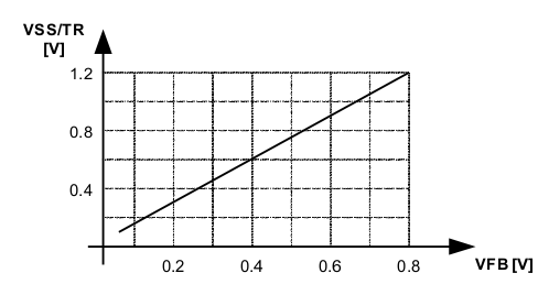 Figure 6. Voltage Tracking Relationship
Once the SS/TR pin voltage reaches about 1.2 V, the internal voltage is clamped to the internal feedback voltage and device goes to normal regulation. This works for rising and falling tracking voltages with the same behavior, as long as the input voltage is inside the recommended operating conditions. For decreasing SS/TR pin voltage, the device does not sink current from the output. So, the resulting decrease of the output voltage may be slower than the SS/TR pin voltage if the load is light. When driving the SS/TR pin with an external voltage, do not exceed the voltage rating of the SS/TR pin which is VIN+0.3 V.
If the input voltage drops into undervoltage lockout or even down to zero, the output voltage will go to zero, independent of the tracking voltage. Figure 7 shows how to connect devices to get ratiometric and simultaneous sequencing by using the tracking function.
spacing
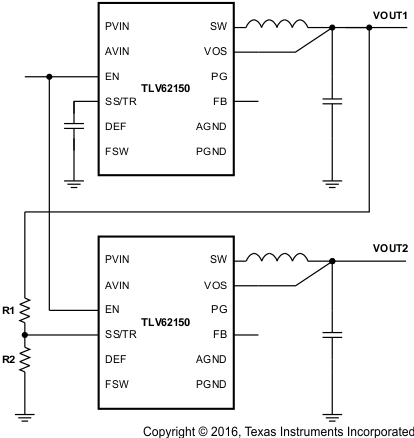 Figure 7. Sequence for Ratiometric and Simultaneous Startup
The resistive divider of R1 and R2 can be used to change the ramp rate of VOUT2 faster, slower or the same as VOUT1.
A sequential startup is achieved by connecting the PG pin of VOUT1 to the EN pin of VOUT2. Ratiometric start up sequence happens if both supplies are sharing the same soft start capacitor. Equation 10 calculates the soft start time, though the SS/TR current has to be doubled. Details about these and other tracking and sequencing circuits are found in SLVA470.
Note: If the voltage at the FB pin is below its typical value of 0.8 V, the output voltage accuracy may have a wider tolerance than specified.
9.2.2.4 Output Filter and Loop Stability
The TLV62150 is internally compensated to be stable with L-C filter combinations corresponding to a corner frequency to be calculated with Equation 12:

Proven nominal values for inductance and ceramic capacitance are given in Table 4 and are recommended for use. Different values may work, but care has to be taken on the loop stability which will be affected. More information including a detailed L-C stability matrix can be found in SLVA463.
The TLV62150 includes an internal 25 pF feedforward capacitor, connected between the VOS and FB pins. This capacitor impacts the frequency behavior and sets a pole and zero in the control loop with the resistors of the feedback divider, per equation Equation 13 and Equation 14:
spacing

spacing

spacing
Though the TLV62150 is stable without the pole and zero being in a particular location, adjusting their location to the specific needs of the application can provide better performance in Power Save mode and/or improved transient response. An external feedforward capacitor can also be added. A more detailed discussion on the optimization for stability versus transient response can be found in SLVA289 and SLVA466.
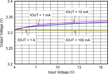
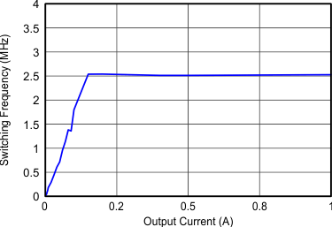
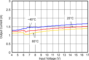
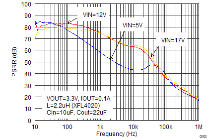
9.2.3 Application Curves
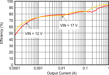
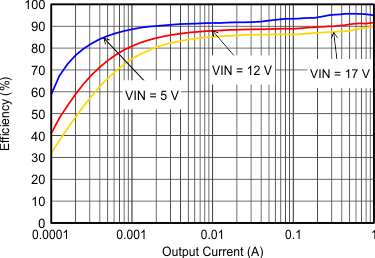
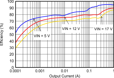
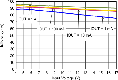
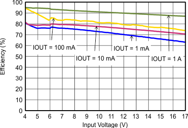
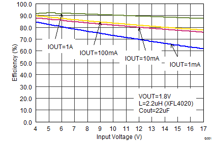
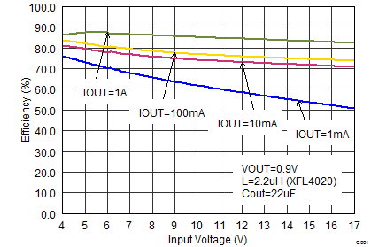
VIN = 12 V, VOUT = 3.3 V, TA = 25°C, (unless otherwise noted)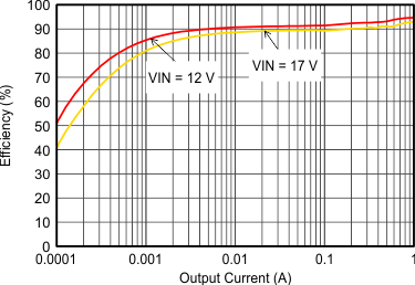
| FSW=Low |
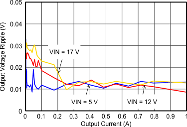
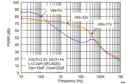
| IOUT = 1 A |
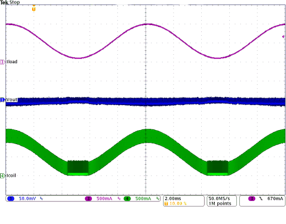 Figure 28. PWM-PSM-Transition
 (VIN = 12 V, VOUT = 3.3 V With 50 mV/div)
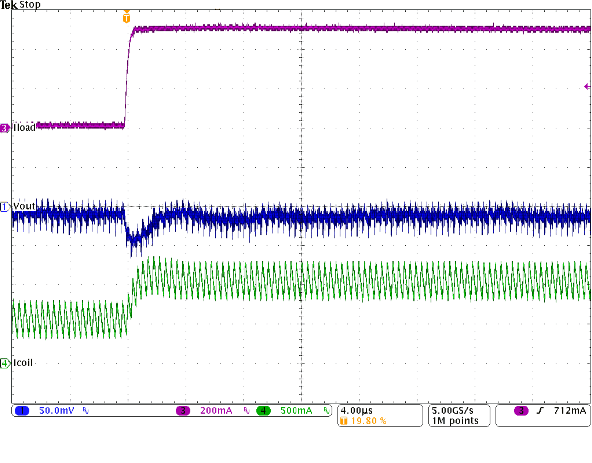 Figure 30. Load Transient Response of Figure 29,
 Rising Edge
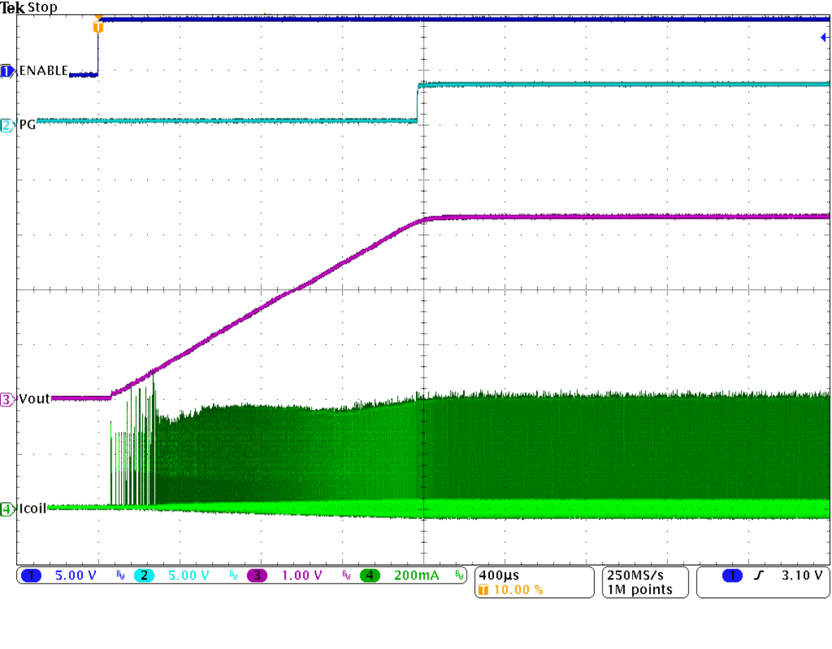 Figure 32. Startup Into 100 mA
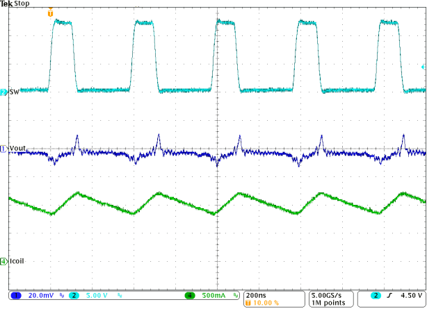 Figure 34. Typical Operation In PWM Mode
 (IOUT = 1 A)
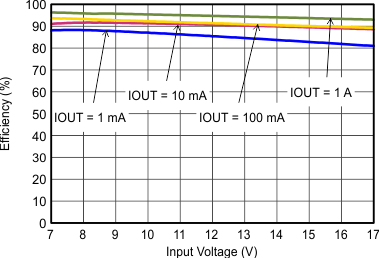
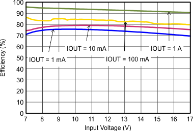
| FSW=Low |
| IOUT = 0.1 A |
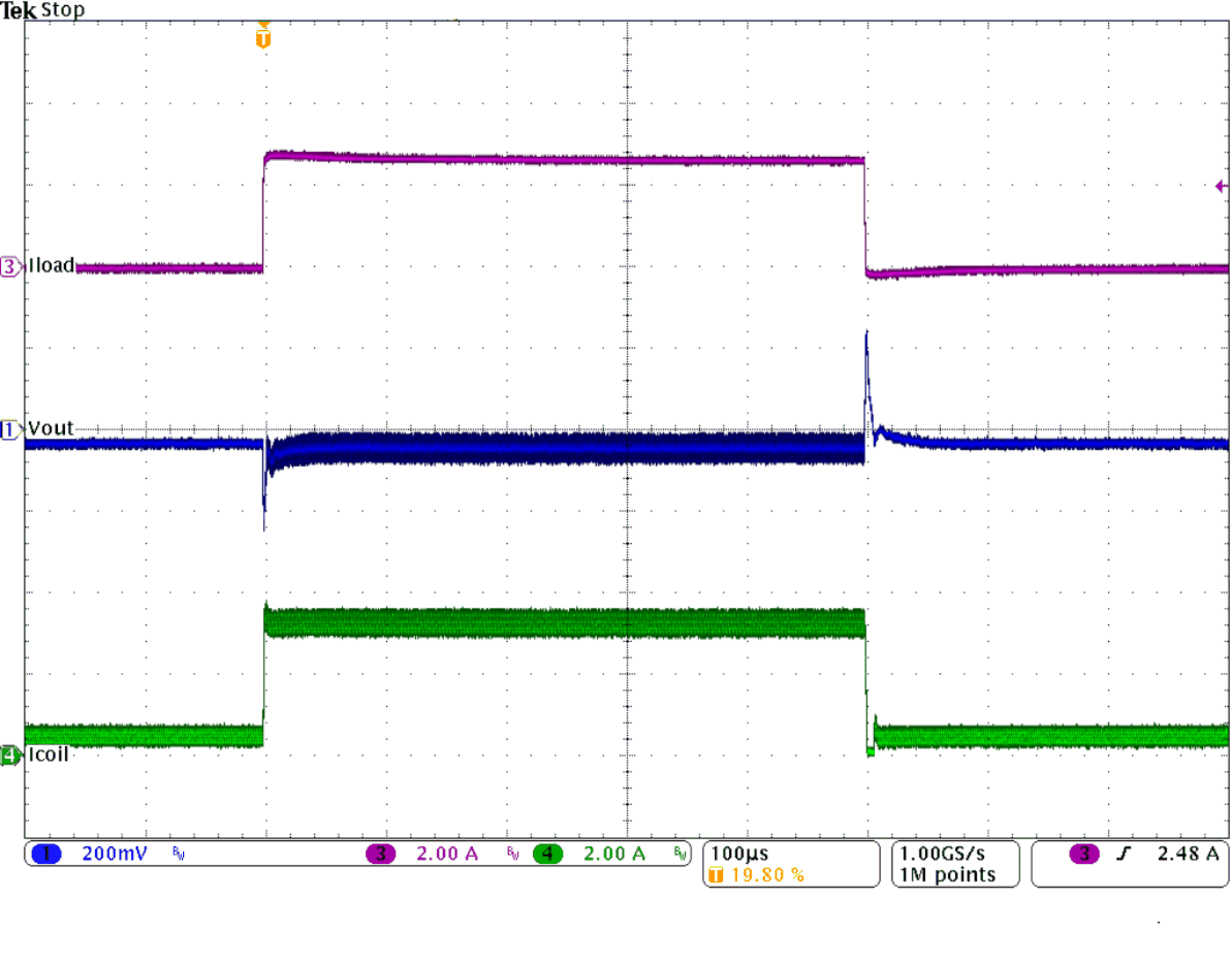 Figure 29. Load Transient Response
 (IOUT= 0.5 to 1 to 0.5 A, VIN = 12 V, VOUT = 3.3 V)
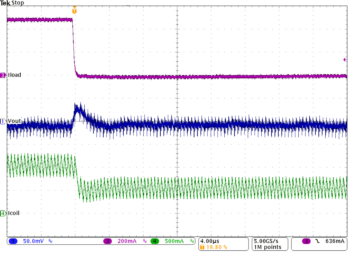 Figure 31. Load Transient Response of Figure 29,
 Falling Edge
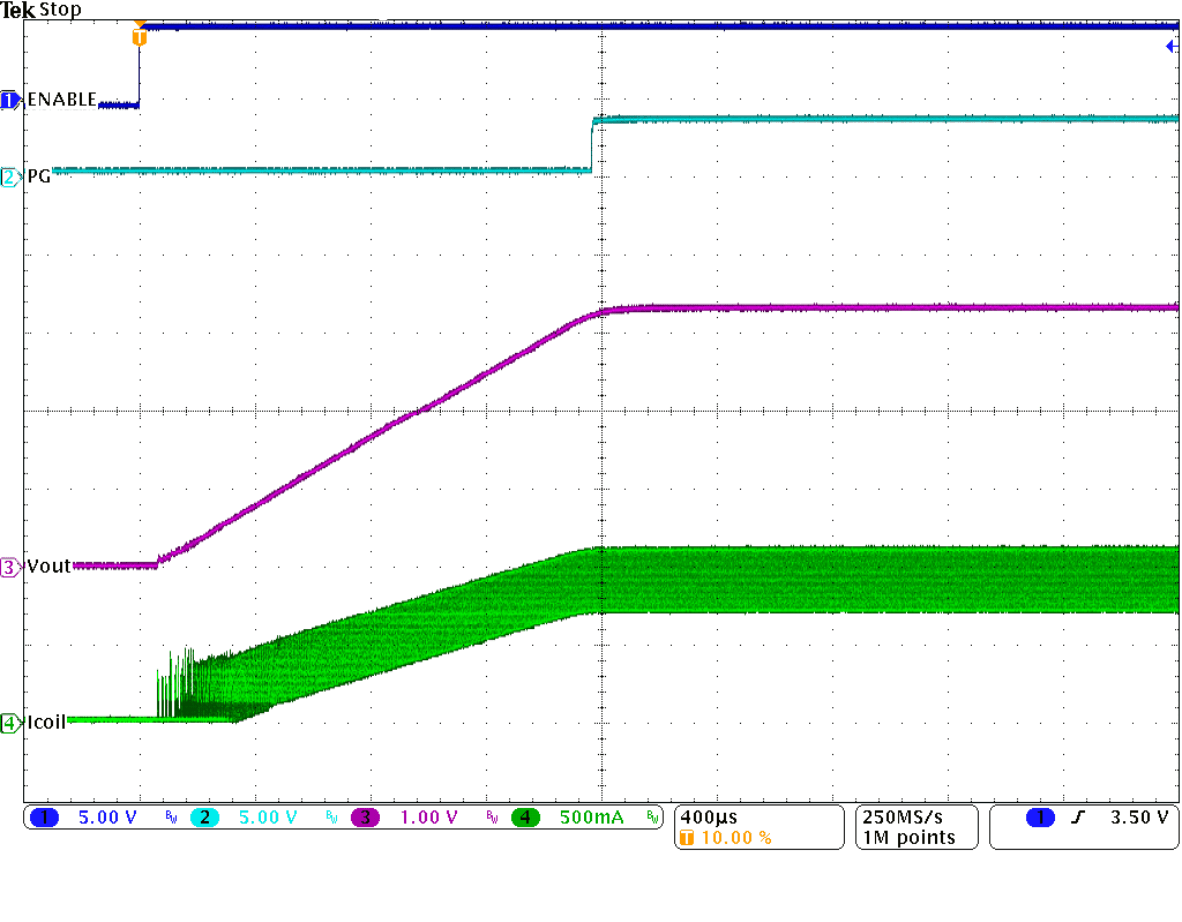 Figure 33. Startup Into 1 A
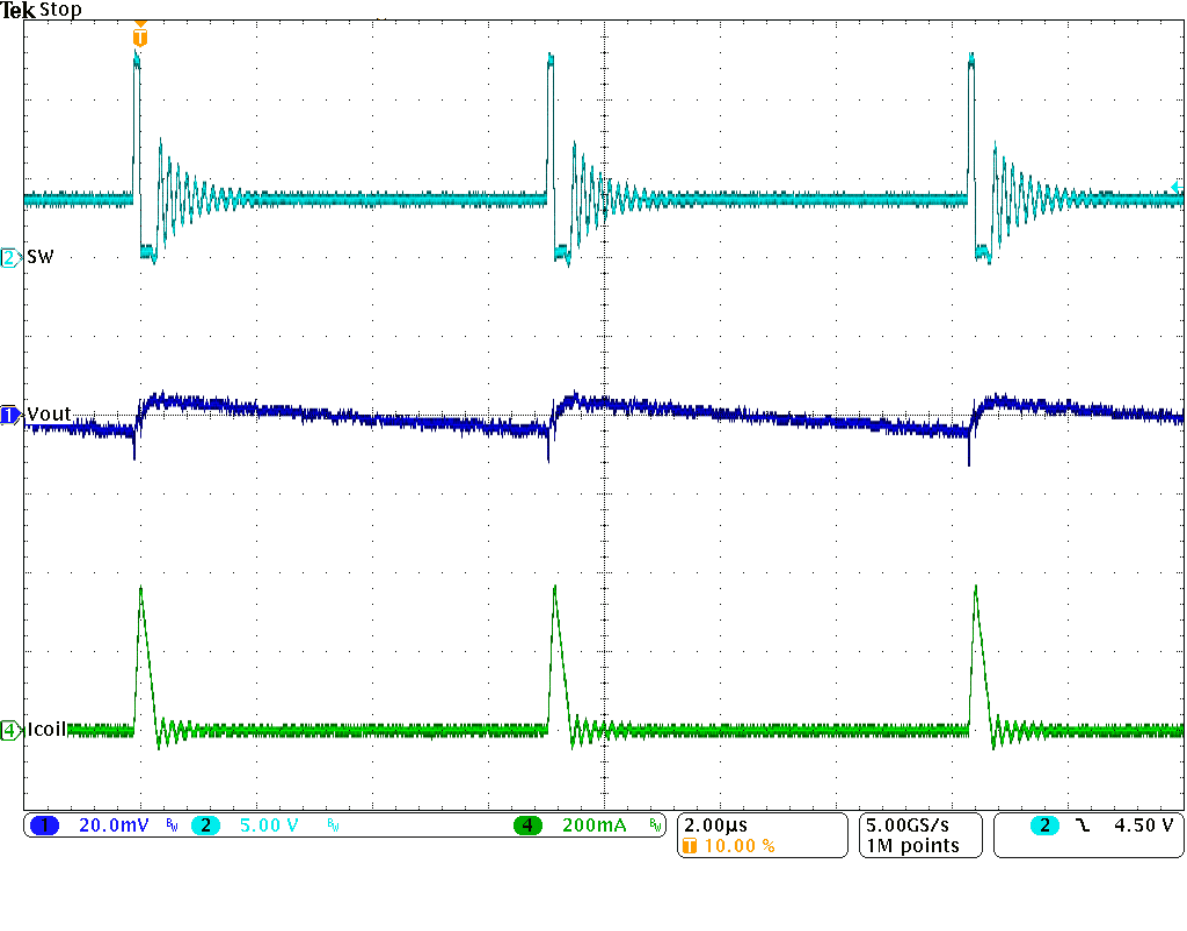 Figure 35. Typical Operation in Power Save Mode
 (IOUT = 10 mA)
9.3 System Examples
9.3.1 LED Power Supply
The TLV62150x can be used as a power supply for power LEDs. The FB pin can be easily set down to lower values than nominal by using the SS/TR pin. With that, the voltage drop on the sense resistor is low to avoid excessive power loss. Since this pin provides 2.5 µA, the FB pin voltage can be adjusted by an external resistor per Equation 15. This drop, proportional to the LED current, is used to regulate the output voltage (anode voltage) to a proper level to drive the LED. Both analog and PWM dimming are supported with the TLV62150. Figure 36 shows an application circuit, tested with analog dimming:
spacing
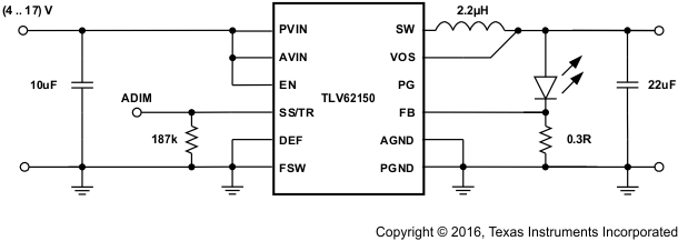 Figure 36. 1-A Single LED Power Supply
spacing
The resistor at SS/TR sets the FB voltage to a level of about 300 mV and is calculated from Equation 15.
spacing

spacing
The device now supplies a constant current, set by the resistor at the FB pin, by regulating the output voltage accordingly. The minimum input voltage has to be rated according the forward voltage needed by the LED used. More information is available in the Application Note SLVA451.
spacing
9.3.2 Active Output Discharge
The TLV62150A pulls the PG pin Low, when the device is shut down by EN, UVLO or thermal shutdown. Connecting PG to Vout through a resistor can be used to discharge Vout in those cases (see Figure 37). The discharge rate can be adjusted by R3, which is also used to pull up the PG pin in normal operation. For reliability, keep the maximum current into the PG pin less than 10 mA.
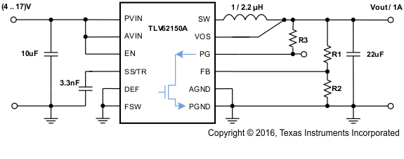 Figure 37. Discharge Vout Through PG Pin with TLV62150A
9.3.3 Inverting Power Supply
The TLV62150 can be used as inverting power supply by rearranging external circuitry as shown in Figure 38. As the former GND node now represents a voltage level below system ground, the voltage difference between VIN and VOUT has to be limited for operation to the maximum supply voltage of 17 V (see Equation 16).
spacing

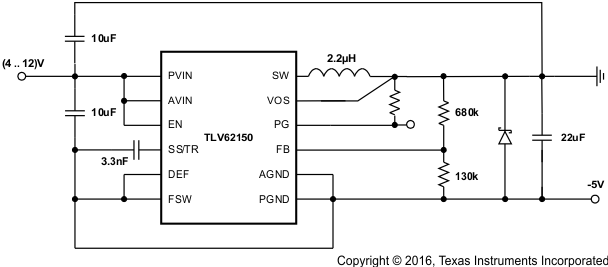 Figure 38. –5-V Inverting Power Supply
spacing
The transfer function of the inverting power supply configuration differs from the buck mode transfer function, incorporating a Right Half Plane Zero additionally. The loop stability has to be adapted and an output capacitance of at least 22 µF is recommended. A detailed design example is given in SLVA469.
spacing
9.3.4 Various Output Voltages
The following example circuits show how to configure the external circuitry to furnish different output voltages at 1 A.
spacing
spacing
 Figure 39. 5-V/1-A Power Supply
spacing
spacing
 Figure 40. 3.3-V/1-A Power Supply
spacing
spacing
 Figure 41. 2.5-V/1-A Power Supply
spacing
spacing
 Figure 42. 1.8-V/1-A Power Supply
spacing
spacing
spacing
spacing
 Figure 43. 1.5-V/1-A Power Supply
spacing
spacing
 Figure 44. 1.2-V/1-A Power Supply
spacing
spacing
 Figure 45. 1-V/1-A Power Supply
spacing