ZHCS792F March   2012  – January 2017 TLV62090

PRODUCTION DATA.  

  1. 特性
  2. 应用范围
  3. 说明
  4. 修订历史记录
  5. Pin Configuration and Functions
  6. Specifications
    1. 6.1 Absolute Maximum Ratings
    2. 6.2 ESD Ratings
    3. 6.3 Recommended Operating Conditions
    4. 6.4 Thermal Information
    5. 6.5 Electrical Characteristics
    6. 6.6 Typical Characteristics
  7. Detailed Description
    1. 7.1 Overview
    2. 7.2 Functional Block Diagram
    3. 7.3 Feature Description
      1. 7.3.1 Enable (EN)
      2. 7.3.2 Softstart (SS) and Hiccup Current Limit During Startup
      3. 7.3.3 Voltage Tracking (SS)
      4. 7.3.4 Short Circuit Protection (Hiccup-Mode)
      5. 7.3.5 Output Discharge Function
      6. 7.3.6 Power Good Output (PG)
      7. 7.3.7 Undervoltage Lockout (UVLO)
      8. 7.3.8 Thermal Shutdown
      9. 7.3.9 Charge Pump (CP, CN)
    4. 7.4 Device Functional Modes
      1. 7.4.1 PWM Operation
      2. 7.4.2 Power Save Mode Operation
      3. 7.4.3 Low Dropout Operation (100% Duty Cycle)
  8. Application and Implementation
    1. 8.1 Application Information
    2. 8.2 Typical Application
      1. 8.2.1 Design Requirements
      2. 8.2.2 Detailed Design Procedure
        1. 8.2.2.1 Custom Design with WEBENCH® Tools
        2. 8.2.2.2 Inductor Selection
        3. 8.2.2.3 Input and Output Capacitor Selection
        4. 8.2.2.4 Setting the Output Voltage
      3. 8.2.3 Application Curves
  9. Power Supply Recommendations
  10. 10Layout
    1. 10.1 Layout Guideline
    2. 10.2 Layout Example
  11. 11器件和文档支持
    1. 11.1 器件支持
      1. 11.1.1 使用 WEBENCH® 工具定制设计方案
    2. 11.2 文档支持
      1. 11.2.1 Third-Party Products Disclaimer
    3. 11.3 接收文档更新通知
    4. 11.4 社区资源
    5. 11.5 商标
    6. 11.6 静电放电警告
    7. 11.7 Glossary
  12. 12机械、封装和可订购信息

Layout

Layout Guideline

  • It is recommended to place the input capacitor as close as possible to the IC pins PVIN and PGND.
  • The VOS connection is noise sensitive and needs to be routed short and direct to the output terminal of the inductor.
  • The exposed thermal pad of the package, analog ground (pin 6) and power ground (pin 14, 15) should have a single point connection at the exposed thermal pad of the package. This minimizes switch node jitter.
  • The charge pump capacitor connected to CP and CN should be placed close to the IC to minimize coupling of switching waveforms into other traces and circuits.
  • See Figure 25 and the evaluation module User Guide (SLVU670) for an example of component placement, routing and thermal design.
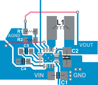
Layout Example

TLV62090 TLV62090_layout.gif Figure 25. Recommended Layout