ZHCS810H January 2012 – February 2018 DS125DF410
PRODUCTION DATA.
- 1 特性
- 2 应用
- 3 说明
- 4 修订历史记录
- 5 Pin Configuration and Functions
- 6 Specifications
-
7 Detailed Description
- 7.1 Overview
- 7.2 Functional Block Diagram
- 7.3 Feature Description
- 7.4 Device Functional Modes
- 7.5
Programming
- 7.5.1 SMBus Strap Observation
- 7.5.2 Device Revision and Device ID
- 7.5.3 Control/Shared Register Reset
- 7.5.4 Interrupt Channel Flag Bits
- 7.5.5 SMBus Master Mode Control Bits
- 7.5.6 Resetting Individual Channels of the Retimer
- 7.5.7 Interrupt Status
- 7.5.8 Overriding the CTLE Boost Setting
- 7.5.9 Overriding the VCO Search Values
- 7.5.10 Overriding the Output Multiplexer
- 7.5.11 Overriding the VCO Divider Selection
- 7.5.12 Using the PRBS Generator
- 7.5.13 Using the Internal Eye Opening Monitor
- 7.5.14 Overriding the DFE Tap Weights and Polarities
- 7.5.15 Enabling Slow Rise/Fall Time on the Output Driver
- 7.5.16 Inverting the Output Polarity
- 7.5.17 Overriding the Figure of Merit for Adaptation
- 7.5.18 Setting the Rate and Subrate for Lock Acquisition
- 7.5.19 Setting the Adaptation/Lock Mode
- 7.5.20 Initiating Adaptation
- 7.5.21 Setting the Reference Enable Mode
- 7.5.22 Overriding the CTLE Settings Used for CTLE Adaptation
- 7.5.23 Setting the Output Differential Voltage
- 7.5.24 Setting the Output De-Emphasis Setting
- 7.6 Register Maps
- 8 Application and Implementation
- 9 Power Supply Recommendations
- 10Layout
- 11器件和文档支持
- 12机械、封装和可订购信息
8.2.3 Application Curves
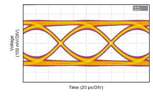
Figure 7 shows a typical output eye diagram for the DS125DF410 operating at 12.5 Gbps with default VOD of 600mVp-p and de-emphasis setting of –2dB.
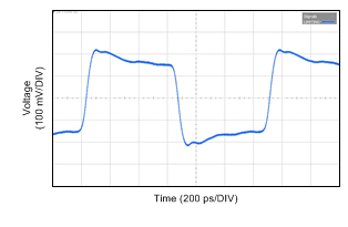
Figure 8 shows an example of Tx de-emphasis for a DS125DF410 operating at 12.5 Gbps. In this example, the high speed output is configured for 600mVp-p VOD and de-emphasis is set to –4.5dB. An 8T pattern is used to evaluate the driver, which consists of 0xFF00.
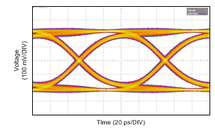
Figure 9 shows a typical output eye diagram for the DS125DF410 operating at 10.3125 Gbps with default VOD of 600mVp-p and de-emphasis setting of –2dB.
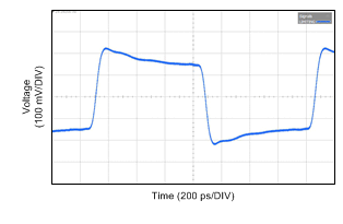
Figure 10 shows an example of Tx de-emphasis for a DS125DF410 operating at 10.3125 Gbps. In this example, the high speed output is configured for 600mVp-p VOD and de-emphasis is set to –4.5dB. An 8T pattern is used to evaluate the driver, which consists of 0xFF00.
 Figure 7. Typical Output Eye Diagram for the DS125DF410 Operating at 12.5 Gbps
 Figure 9. Typical Output Eye Diagram for the DS125DF410 Operating at 10.3125 Gbps with Default VOD of 600mVp-p and De-emphasis Setting of –2dB
 Figure 8. Example of Tx De-emphasis for a DS125DF410 Operating at 12.5 Gbps
 Figure 10. Example Of Tx De-emphasis for a DS125DF410 Operating at 10.3125 Gbps