ZHCS862E March 2012 – May 2017 TPS62125
PRODUCTION DATA.
- 1 特性
- 2 应用
- 3 说明
- 4 修订历史记录
- 5 Pin Configuration and Functions
- 6 Specifications
- 7 Detailed Description
- 8 Application and Implementation
- 9 Power Supply Recommendations
- 10Layout
- 11器件和文档支持
- 12机械、封装和可订购信息
8 Application and Implementation
NOTE
Information in the following applications sections is not part of the TI component specification, and TI does not warrant its accuracy or completeness. TI’s customers are responsible for determining suitability of components for their purposes. Customers should validate and test their design implementation to confirm system functionality.
8.1 Application Information
The TPS62125 is a high-efficiency synchronous step-down converter providing a wide output voltage range from 1.2 V to 10 V.
8.2 Typical Application
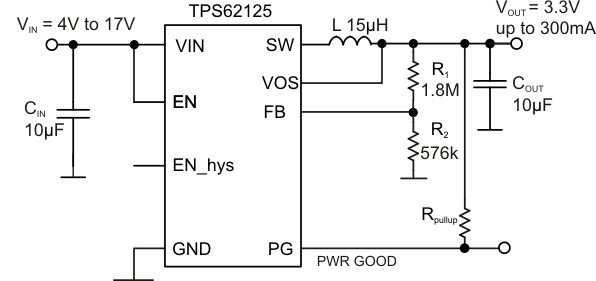 Figure 8. TPS62125 3.3-V Output Voltage Configuration
8.2.1 Design Requirements
The device operates over an input voltage range from 3 V to 17 V. The output voltage is adjustable using an external feedback divider.
8.2.2 Detailed Design Procedure
8.2.2.1 Output Voltage Setting
The output voltage can be calculated by:
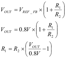
The internal reference voltage for the error amplifier, VREF_FB, is nominal 0.808 V. However for the feedback resistor divider selection, it is recommended to use the value 0.800 V as the reference. Using this value, the output voltage sets 1% higher and provides more headroom for load transients as well for line and load regulation. The current through the feedback resistors R1 and R2 should be higher than 1 µA. In applications operating over full temperature range or in noisy environments, this current may be increased for robust operation. However, higher currents through the feedback resistors impact the light load efficiency of the converter.
Table 1 shows a selection of suggested values for the feedback divider network for most common output voltages.
Table 1. Suggested Values for Feedback Divider Network
| OUTPUT VOLTAGE | 1.2 V | 1.8 V | 3.3 V | 5 V | 6.7 V | 8 V |
|---|---|---|---|---|---|---|
| R1 [kΩ] | 180 | 300 | 1800 | 1100 | 1475 | 1800 |
| R2 [kΩ] | 360 | 240 | 576 | 210 | 200 | 200 |
8.2.2.2 Enable Threshold and Hysteresis Setting
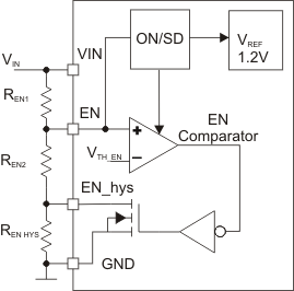 Figure 9. Using the Enable Comparator Threshold and Hysteresis for an Input SVS (Supply Voltage Supervisor)
The enable comparator can be used as an adjustable input supply voltage supervisor (SVS) to start and stop the DC/DC converter depending on the input voltage level. The input voltage level, VIN_startup, at which the device starts up is set by the resistors REN1 and REN2 and can be calculated by :

The resistor values REN1 and REN2 can be calculated by:


The input voltage level VIN_stop at which the device will stop operation is set by REN1, REN2 and REN HYS and can be calculated by:

The resistor value REN_hys can be calculated according to:

The current through the resistors REN1, REN2, and REN HYS should be higher than 1 µA. In applications operating over the full temperature range and in noisy environments, the resistor values can be reduced to smaller values.
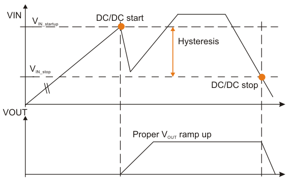 Figure 10. Using the EN Comparator as Input SVS for Proper VOUT Ramp Up
8.2.2.3 Power Good (PG) Pullup and Output Discharge Resistor
The power good open collector output needs an external pull up resistor to indicate a high level. The pull up resistor can be connected to a voltage level up to 10 V. The output can sink current up to 0.4 mA with specified output low level of less than 0.3 V. The lowest value for the pull up resistor can be calculated by:

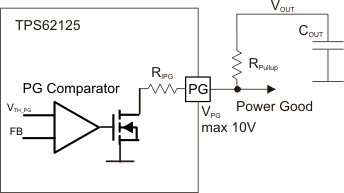 Figure 11. PG Open Collector Output
The PG pin can be used to discharge the output capacitor. The PG output has an internal resistance RIPG of typical 600 Ω and minimum 400 Ω. The maximum sink current into the PG pin is 10 mA. In order to limit the discharge current to the maximum allowable sink current into the PG pin, the external pull up resistor RPull up can be calculated to:

In case a negative value is calculated, the external pull up resistor can be removed and the PG pin can be directly connected to the output.
8.2.2.4 Output Filter Design (Inductor and Output Capacitor)
The external components have to fulfill the needs of the application, but also the stability criteria of the devices control loop. The TPS62125 is optimized to work within a range of L and C combinations. The LC output filter inductance and capacitance have to be considered together, creating a double pole, responsible for the corner frequency of the converter. Table 2 can be used to simplify the output filter component selection.
Table 2. Recommended LC Output Filter Combinations
| INDUCTOR VALUE [µH](2) | OUTPUT CAPACITOR VALUE [µF](1) | |||
|---|---|---|---|---|
| 10 µF | 2 x 10 µF | 22 µF | 47 µF | |
| VOUT 1.2 V - 1.8 V | ||||
| 15 | √ | √ | √ | √ |
| 22 | √(3) | √ | √ | √ |
| VOUT 1.8 V - 3.3 V | ||||
| 15 | √(3) | √ | √ | √ |
| 22 | √(3) | √ | √ | √ |
| VOUT 3.3 V - 5 V | ||||
| 10 | √ | √ | √ | |
| 15 | √(3) | √(3) | √ | |
| 22 | ||||
| VOUT 5 V - 10 V | ||||
| 10 | √(3) | √(3) | √ | |
| 15 | √ | √ | √ | |
| 22 | √ | √ | √ | |
More detailed information on further LC combinations can be found in application note SLVA515.
8.2.2.5 Inductor Selection
The inductor value affects its peak-to-peak ripple current, the PWM-to-PFM transition point, the output voltage ripple and the efficiency. The selected inductor has to be rated for its DC resistance and saturation current. The inductor ripple current (ΔIL) decreases with higher inductance and increases with higher VIN or VOUT and can be estimated according to Equation 13.
Equation 14 calculates the maximum inductor current under static load conditions. The saturation current of the inductor should be rated higher than the maximum inductor current as calculated with Equation 14. This is recommended because during heavy load transient the inductor current will rise above the calculated value. A more conservative way is to select the inductor saturation current according to the high-side MOSFET switch current limit ILIMF.


where
- TON: See Equation 1
- L: Inductance
- ΔIL: Peak to Peak inductor ripple current
- ILmax: Maximum Inductor current
In DC/DC converter applications, the efficiency is essentially affected by the inductor AC resistance (i.e. quality factor) and by the inductor DCR value. To achieve high-efficiency operation, take care in selecting inductors featuring a quality factor above 25 at the switching frequency. Increasing the inductor value produces lower RMS currents, but degrades transient response. For a given physical inductor size, increased inductance usually results in an inductor with lower saturation current.
The total losses of the coil consist of both the losses in the DC resistance (RDC) and the following frequency-dependent components:
- The losses in the core material (magnetic hysteresis loss, especially at high switching frequencies)
- Additional losses in the conductor from the skin effect (current displacement at high frequencies)
- Magnetic field losses of the neighboring windings (proximity effect)
- Radiation losses
The following inductor series from different suppliers have been used with the TPS62125.
Table 3. List of Inductors
| INDUCTANCE [µH] | DCR [Ω] | DIMENSIONS [mm3] | INDUCTOR TYPE | SUPPLIER |
|---|---|---|---|---|
| 10 / 15 | 0.33 max / 0.44 max. | 3.3 x 3.3 x 1.4 | LPS3314 | Coilcraft |
| 22 | 0.36 max. | 3.9 x 3.9 x 1.8 | LPS4018 | Coilcraft |
| 15 | 0.33 max. | 3.0 x 2.5 x 1.5 | VLF302515 | TDK |
| 10/15 | 0.44 max / 0.7 max. | 3.0 x 3.0 x 1.5 | LPS3015 | Coilcraft |
| 10 | 0.38 typ. | 3.2 × 2.5 × 1.7 | LQH32PN | Murata |
8.2.2.6 Output Capacitor Selection
Ceramic capacitors with low ESR values provide the lowest output voltage ripple and are recommended. The output capacitor requires either an X7R or X5R dielectric. Y5V and Z5U dielectric capacitors, aside from their wide variation in capacitance over temperature, become resistive at high frequencies.
At light load currents the converter operates in power-save mode and the output voltage ripple is dependent on the output capacitor value and the PFM peak inductor current. Higher output capacitor values minimize the voltage ripple in PFM Mode and tighten DC output accuracy in PFM mode. In order to achieve specified regulation performance and low-output voltage ripple, the DC-bias characteristic of ceramic capacitors must be considered. The effective capacitance of ceramic capacitors drops with increasing DC-bias voltage. Due to this effect, it is recommended for output voltages above 3.3 V to use at least 1 x 22-µF or 2 x 10-µF ceramic capacitors on the output.
8.2.2.7 Input Capacitor Selection
Because of the nature of the buck converter having a pulsating input current, a low ESR input capacitor is required for best input voltage filtering and minimizing the interference with other circuits caused by high input voltage spikes. For most applications, a 10-µF ceramic capacitor is recommended. The voltage rating and DC bias characteristic of ceramic capacitors need to be considered. The input capacitor can be increased without any limit for better input voltage filtering.
For applications powered from high impedance sources, a tantalum polymer capacitor should be used to buffer the input voltage for the TPS62125. Tantalum polymer capacitors provide a constant capacitance vs. DC bias characteristic compared to ceramic capacitors. In this case, a 10-µF ceramic capacitor should be used in parallel to the tantalum polymer capacitor to provide low ESR.
Take care when using only small ceramic input capacitors. When a ceramic capacitor is used at the input and the power is being supplied through long wires, such as from a wall adapter, a load step at the output or VIN step on the input can induce large ringing at the VIN pin. This ringing can couple to the output and be mistaken as loop instability or could even damage the part by exceeding the maximum ratings. In case the power is supplied via a connector e.g. from a wall adapter, a hot-plug event can cause voltage overshoots on the VIN pin exceeding the absolute maximum ratings and can damage the device, too. In this case a tantalum polymer capacitor or overvoltage protection circuit reduces the voltage overshoot, see Figure 45.
Table 4 shows a list of input/output capacitors.
Table 4. List of Capacitors
| CAPACITANCE [µF] | SIZE | CAPACITOR TYPE | USAGE | SUPPLIER |
|---|---|---|---|---|
| 10 | 0805 | GRM21B 25V X5R | CIN /COUT | Murata |
| 10 | 0805 | GRM21B 16V X5R | COUT | Murata |
| 22 | 1206 | GRM31CR61 16V X5R | COUT | Murata |
| 22 | B2 (3.5x2.8x1.9) | 20TQC22MYFB | CIN / input protection | Sanyo |
.
8.2.3 Application Curves
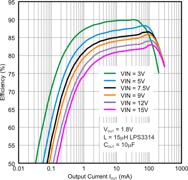 Figure 12. Efficiency vs. Output Current VOUT = 1.8 V
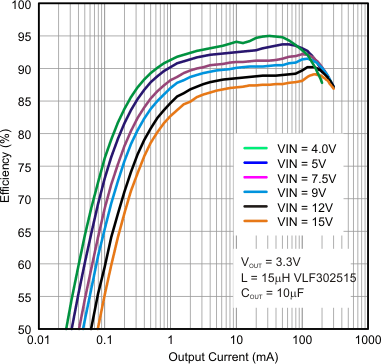 Figure 14. Efficiency vs. Output current, VOUT = 3.3 V
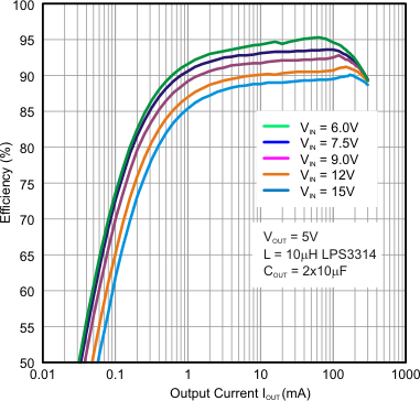 Figure 16. Efficiency vs. Output Current, VOUT = 5 V
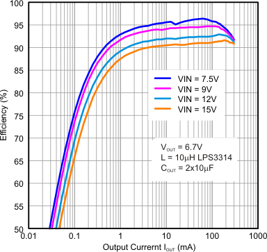 Figure 18. Efficiency vs. Output current, VOUT = 6.8 V
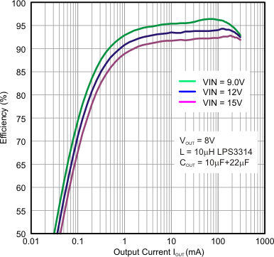 Figure 20. Efficiency vs. Output Current, VOUT = 8 V
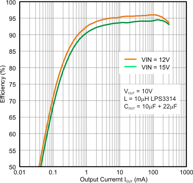 Figure 22. Efficiency vs. Output Current, VOUT = 10 V
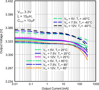 Figure 24. Output Voltage vs. Output Current, VOUT = 3.3 V
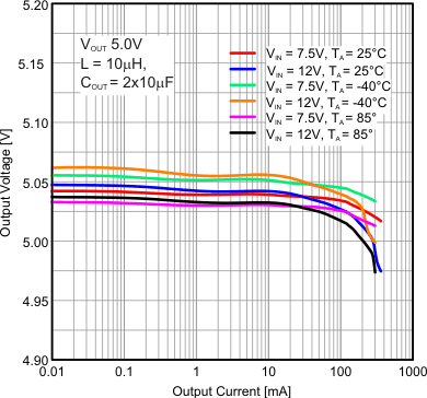 Figure 26. Output Voltage vs. Output current, VOUT = 5 V
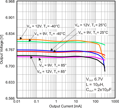 Figure 28. Output Voltage vs. Output Current, VOUT = 6.7 V
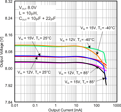 Figure 30. Output Voltage vs. Output Current, VOUT = 8 V
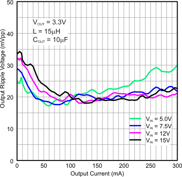 Figure 32. Output Ripple Voltage vs. Output Current,
 VOUT = 3.3 V
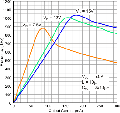 Figure 34. Switch Frequency vs. Output Current, VOUT 5 V
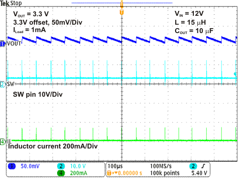 Figure 36. Power-Save Mode VOUT= 3.3 V, IOUT = 1 mA
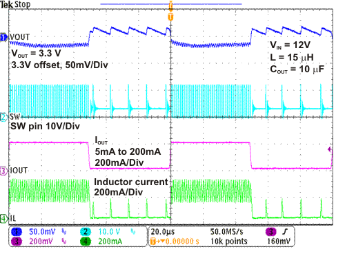 Figure 38. Load Transient 5 mA to 200 mA, VOUT = 3.3 V
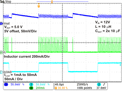 Figure 40. Load Transient 1 mA to 50 mA, VOUT = 5 V
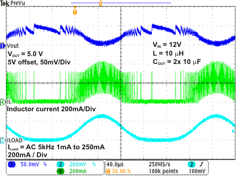 Figure 42. AC Load Regulation VOUT = 5 V
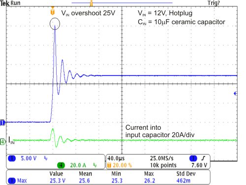 Figure 44. VIN Hotplug Overshoot
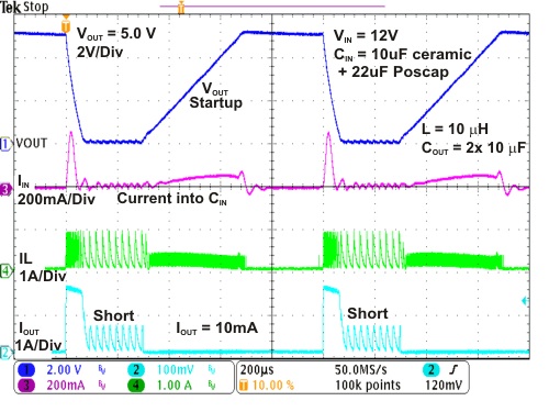 Figure 46. Short Circuit and Overcurrent Protection
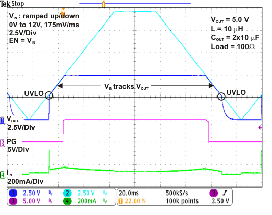 Figure 48. Operation With EN = VIN, VIN Tracks VOUT
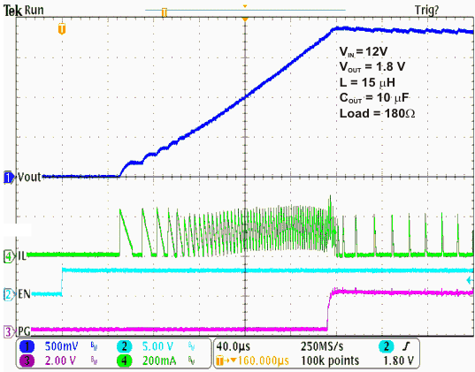 Figure 50. Start-Up 1.8 V VOUT
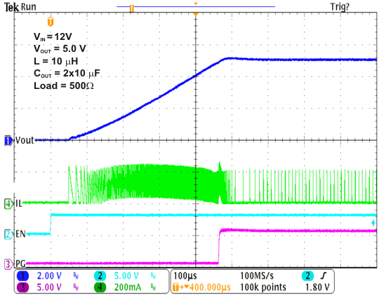 Figure 52. Start-Up 5 V VOUT
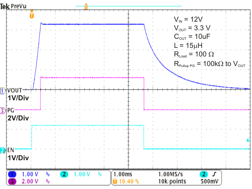 Figure 54. VOUT Ramp Up/Down With EN On/Off
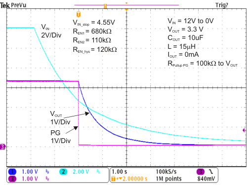 Figure 56. VOUT Ramp Down With Falling VIN, See Schematic Figure 59
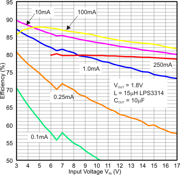 Figure 13. Efficiency vs. Input Voltage, VOUT = 1.8 V
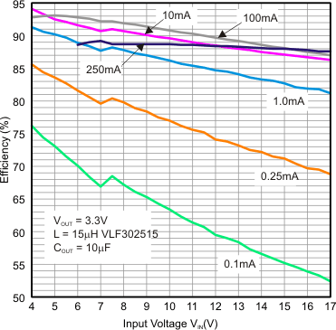 Figure 15. Efficiency vs. Input voltage, VOUT = 3.3 V
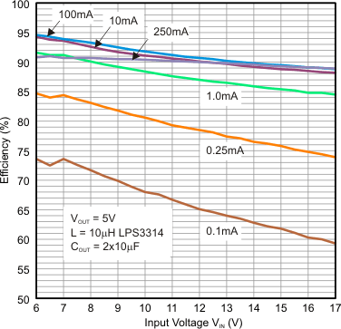 Figure 17. Efficiency vs. Input Voltage, VOUT = 5 V
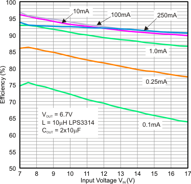 Figure 19. Efficiency vs. Input Voltage, VOUT = 6.8 V
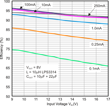 Figure 21. Efficiency vs. Input Voltage, VOUT = 8 V
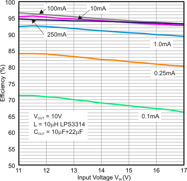 Figure 23. Efficiency vs. Input Voltage, VOUT = 10 V
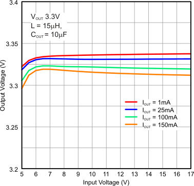 Figure 25. Output Voltage vs. Input Voltage, VOUT = 3.3 V
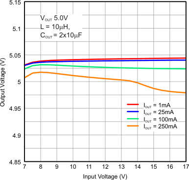 Figure 27. Output Voltage vs. Input Voltage, VOUT = 5 V
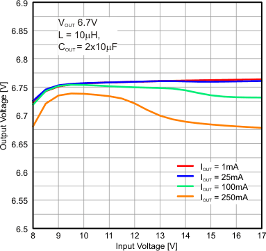 Figure 29. Output voltage vs. Input voltage, VOUT = 6.7 V
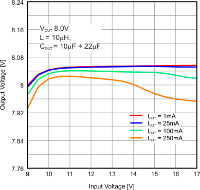 Figure 31. Output Voltage vs. Input Voltage, VOUT = 8 V
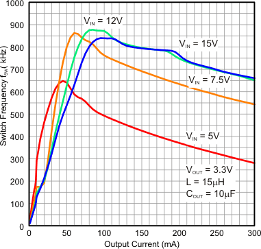 Figure 33. Switch Frequency vs. Output Current,
 VOUT = 3.3 V
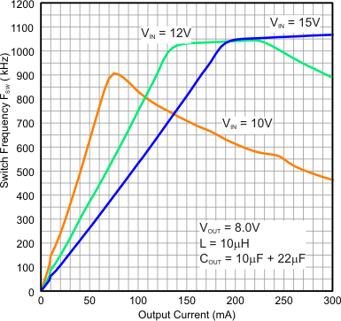 Figure 35. Switch Frequency vs. Output Current, VOUT = 8 V
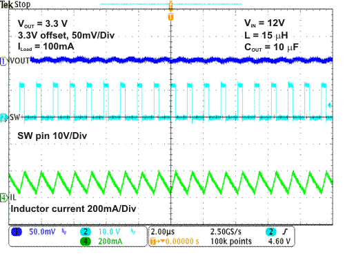 Figure 37. PWM Mode VOUT= 3.3 V, IOUT = 100 mA
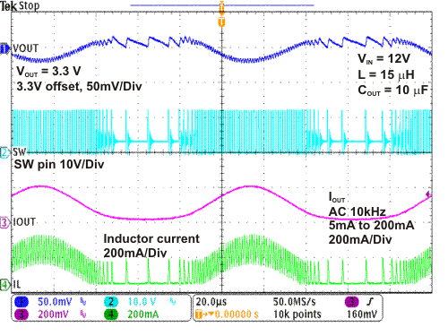 Figure 39. AC Load Regulation, VOUT = 3.3 V
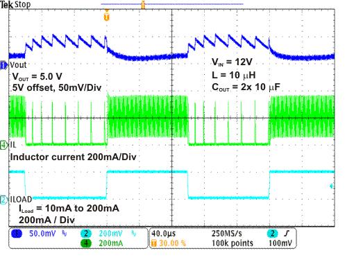 Figure 41. Load Transient 10 mA to 200 mA, VOUT = 5 V
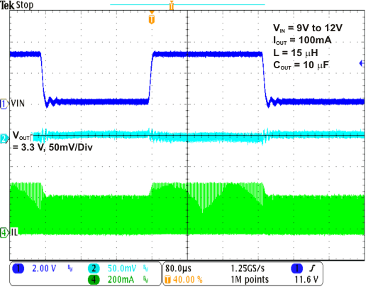 Figure 43. Line Transient Response VIN = 9 V to 12 V
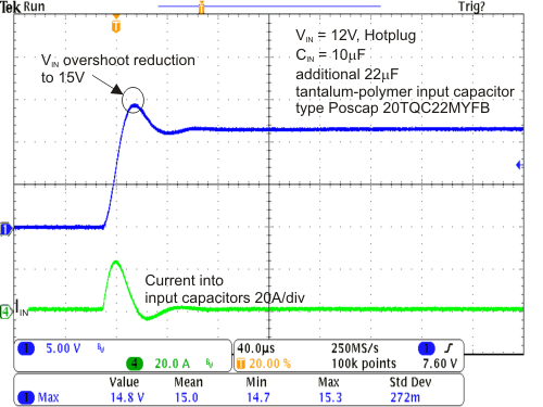 Figure 45. VIN Hotplug Overshoot Reduction With Poscap
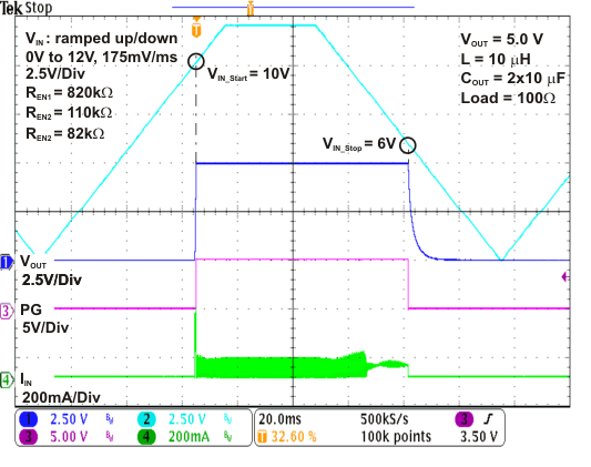 Figure 47. Input Supply Voltage Supervisor (SVS),
 VOUT = 5 V
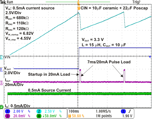 Figure 49. 0.5 mA Current Source, 20 mA Pulse Load
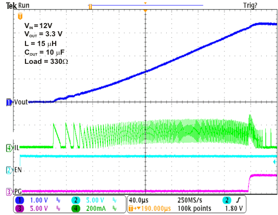 Figure 51. Start-Up 3.3 V VOUT
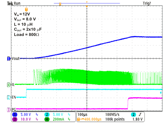 Figure 53. Start-Up 8 V VOUT
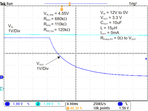 Figure 55. Output Discharge Using PG Pin, Triggered by EN Comparator
8.3 System Examples
8.3.1 TPS62125 5-V Output Voltage Configuration
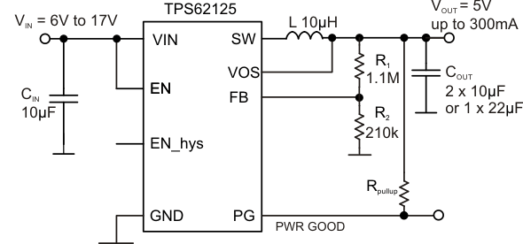 Figure 57. TPS62125 5-V Output Voltage Configuration
8.3.2 TPS62125 5-V VOUT
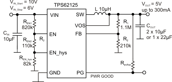 Figure 58. TPS62125 5-V VOUT, Start-up Voltage VIN_Start = 10 V, Stop Voltage VIN_Stop = 6 V, See Figure 47
8.3.3 TPS62125 Operation From a Storage Capacitor Charged From a 0.5 mA Current Source
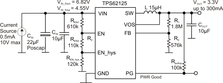 Figure 59. TPS62125 Operation From a Storage Capacitor Charged From a 0.5 mA Current Source,
 VOUT = 3.3 V, See Figure 49
8.3.4 5 V to –5 V Inverter Configuration
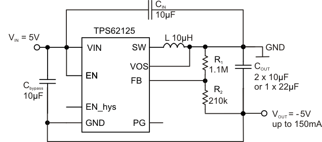 Figure 60. 5 V to –5 V Inverter Configuration, See SLVA514