ZHCS901E May 2012 – September 2021 TPS55340
PRODUCTION DATA
- 1 特性
- 2 应用
- 3 说明
- 4 Revision History
- 5 Pin Configuration and Functions
- 6 Specifications
- 7 Detailed Description
-
8 Application and Implementation
- 8.1 Application Information
- 8.2
Typical Applications
- 8.2.1
Boost Converter
- 8.2.1.1 Design Requirements
- 8.2.1.2
Detailed Design Procedure
- 8.2.1.2.1 Custom Design with WEBENCH Tools
- 8.2.1.2.2 Selecting the Switching Frequency (R4)
- 8.2.1.2.3 Determining the Duty Cycle
- 8.2.1.2.4 Selecting the Inductor (L1)
- 8.2.1.2.5 Computing the Maximum Output Current
- 8.2.1.2.6 Selecting the Output Capacitors (C8, C9, C10)
- 8.2.1.2.7 Selecting the Input Capacitors (C2, C7)
- 8.2.1.2.8 Setting Output Voltage (R1, R2)
- 8.2.1.2.9 Setting the Soft-start Time (C7)
- 8.2.1.2.10 Selecting the Schottky Diode (D1)
- 8.2.1.2.11 Compensating the Control Loop (R3, C4, C5)
- 8.2.1.3 Application Curves
- 8.2.2
SEPIC Converter
- 8.2.2.1 Design Requirements
- 8.2.2.2
Detailed Design Procedure
- 8.2.2.2.1 Selecting the Switching Frequency (R4)
- 8.2.2.2.2 Duty Cycle
- 8.2.2.2.3 Selecting the Inductor (L1)
- 8.2.2.2.4 Calculating the Maximum Output Current
- 8.2.2.2.5 Selecting the Output Capacitors (C8, C9, C10)
- 8.2.2.2.6 Selecting the Series Capacitor (C6)
- 8.2.2.2.7 Selecting the Input Capacitor (C2, C7)
- 8.2.2.2.8 Selecting the Schottky Diode (D1)
- 8.2.2.2.9 Setting the Output Voltage (R1, R2)
- 8.2.2.2.10 Setting the Soft-start Time (C3)
- 8.2.2.2.11 MOSFET Rating Considerations
- 8.2.2.2.12 Compensating the Control Loop (R3, C4)
- 8.2.2.3 Application Curves
- 8.2.1
Boost Converter
- 9 Power Supply Recommendations
- 10Layout
- 11Device and Documentation Support
- 12Mechanical, Packaging, and Orderable Information
6.6 Typical Characteristics
VIN = 5 V, TA = 25°C (unless otherwise noted)
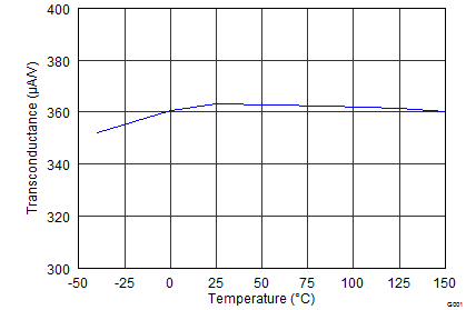 Figure 6-1 Error Amplifier Transconductance vs Temperature
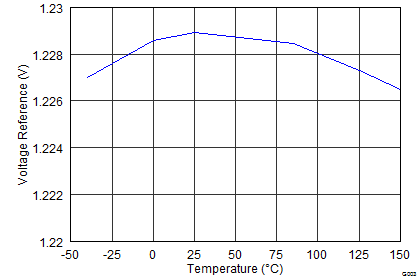 Figure 6-3 Feedback Voltage Reference vs Temperature
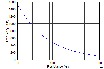 Figure 6-5 Frequency vs FREQ Resistance
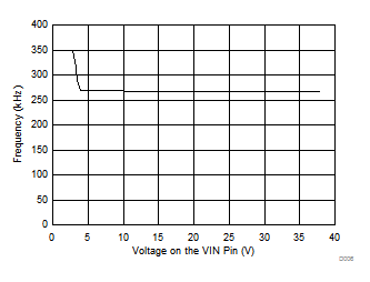 Figure 6-7 Minimum Switching Frequency for Quick Recovery from Frequency Foldback
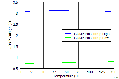 Figure 6-9 COMP Clamp Voltage vs Temperature
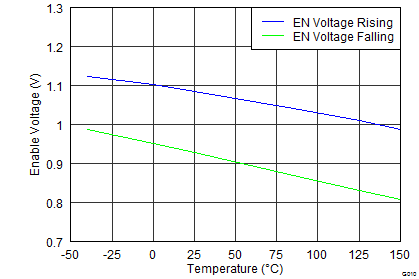 Figure 6-11 Enable Voltage vs Temperature
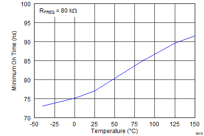 Figure 6-13 Minimum On-Time vs Temperature
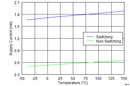 Figure 6-15 Supply Current vs Temperature
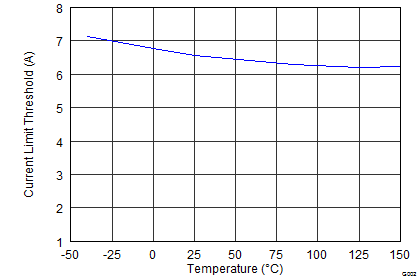 Figure 6-2 Switch Current Limit vs Temperature
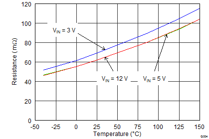 Figure 6-4 RDS(ON) vs Temperature
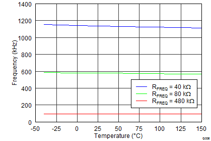 Figure 6-6 Frequency vs Temperature
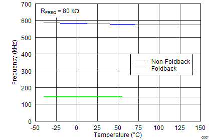 Figure 6-8 Nonfoldback Frequency vs Foldback Frequency
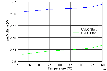 Figure 6-10 Input Voltage UVLO vs Temperature
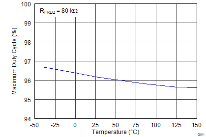 Figure 6-12 Maximum Duty Cycle vs Temperature
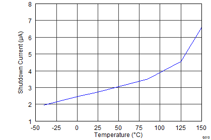 Figure 6-14 Shutdown Current vs Temperature