ZHCS996D June 2012 – February 2018 TPS81256
PRODUCTION DATA.
- 1 特性
- 2 应用
- 3 说明
- 4 修订历史记录
- 5 Device Options
- 6 Pin Configuration and Functions
- 7 Specifications
- 8 Detailed Description
- 9 Application and Implementation
- 10Power Supply Recommendations
- 11Layout
- 12器件和文档支持
- 13机械、封装和可订购信息
7.6 Typical Characteristics
Table 1. Table of Graphs
| FIGURE | |||
|---|---|---|---|
| η | Efficiency | vs Output current | Figure 1, Figure 3 |
| vs Input voltage | Figure 2 | ||
| VO | DC output voltage | vs Output current | Figure 4, Figure 5, Figure 6 |
| vs Input voltage | Figure 7 | ||
| IO | Maximum output current | vs Input voltage | Figure 8 |
| ΔVO | Peak-to-peak output ripple voltage | vs Output current | Figure 8 |
| ICC | Supply current | vs Input voltage | Figure 10 |
| ILIM | Input current | vs Output current | Figure 11 |
Table 2. Table of Animated Performance Characteristics
| VIDEO | |||
|---|---|---|---|
| AC Load Response | vs. Input Voltage | Video 1 | |
| Load Transient Response (10mA to 400mA) | vs. Input Voltage | Video 2 | |
| Load Transient Response (to 400mA) | vs. Base Load Current (2.9VIN) | Video 3 | |
| vs. Base Load Current (3.6VIN) | Video 4 | ||
| vs. Base Load Current (4.2VIN) | Video 5 | ||
| Start-Up Response | vs. Delay to Load Current (2.9VIN) | Video 6 | |
| vs. Delay to Load Current (3.6VIN) | Video 7 | ||
| vs. Delay to Load Current (4.2VIN) | Video 8 | ||
| Start-Up Response (200mA IOUT) | vs. Input Voltage | Video 9 | |
| Overload Response | vs. Input Voltage | Video 10 | |
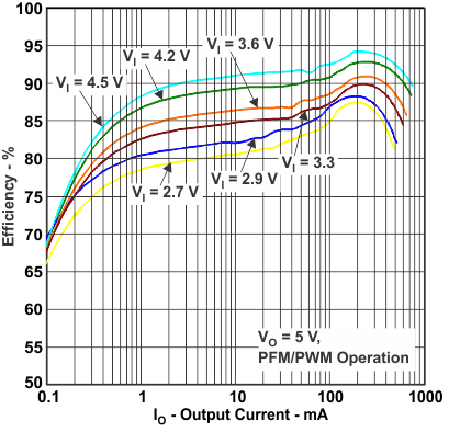 Figure 1. Efficiency vs Output Current
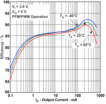 Figure 3. Efficiency vs Output Current
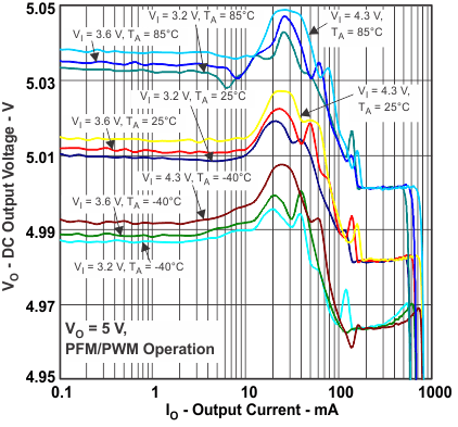 Figure 5. DC Output Voltage vs Output Current
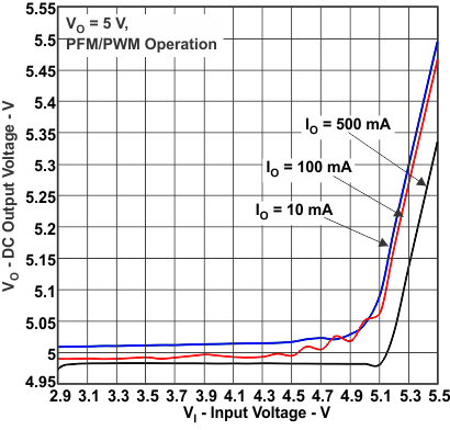 Figure 7. DC Output Voltage vs Input Voltage
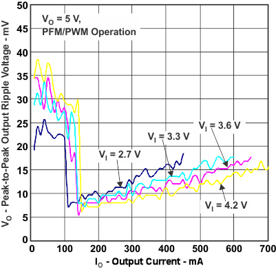 Figure 9. Peak-To-Peak Output Ripple Voltage vs Output Current
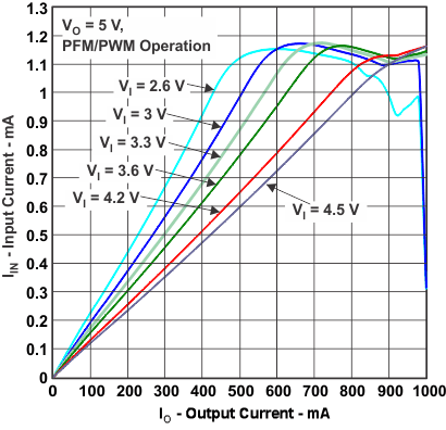
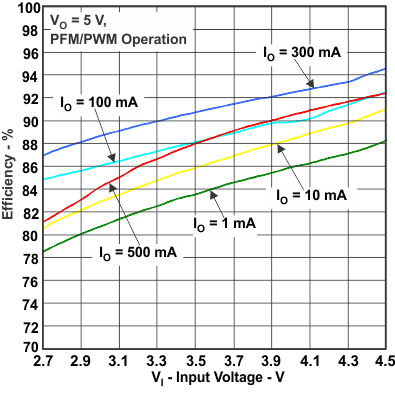 Figure 2. Efficiency vs Input Voltage
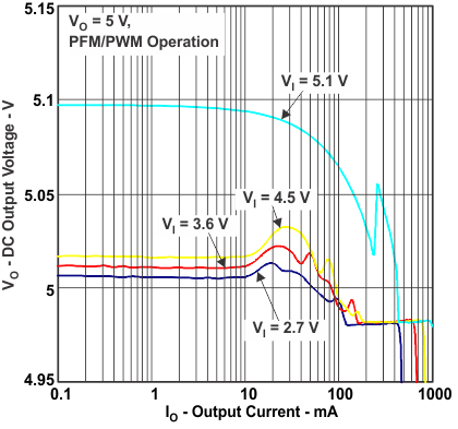 Figure 4. DC Output Voltage vs Output Current
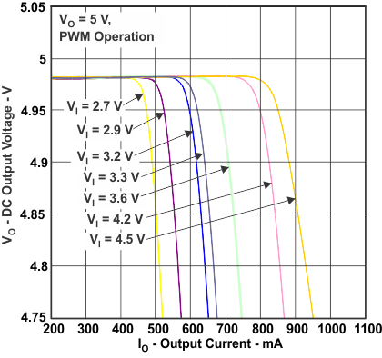 Figure 6. DC Output Voltage vs Output Current
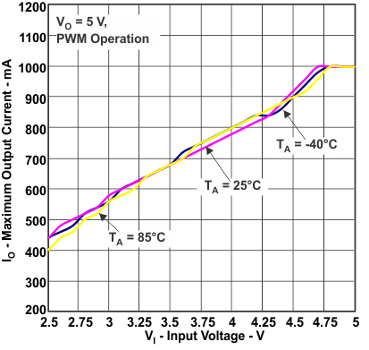 Figure 8. Maximum Output Current vs Input Voltage
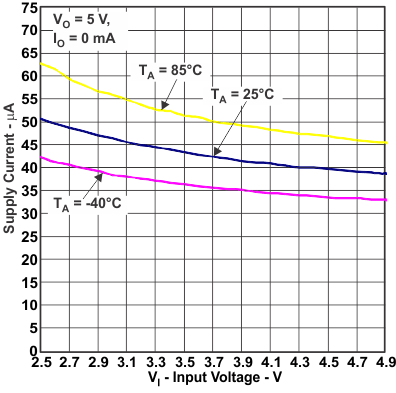 Figure 10. Supply Current vs Input Voltage