ZHCS996D June 2012 – February 2018 TPS81256
PRODUCTION DATA.
- 1 特性
- 2 应用
- 3 说明
- 4 修订历史记录
- 5 Device Options
- 6 Pin Configuration and Functions
- 7 Specifications
- 8 Detailed Description
- 9 Application and Implementation
- 10Power Supply Recommendations
- 11Layout
- 12器件和文档支持
- 13机械、封装和可订购信息
11.2 Layout Example
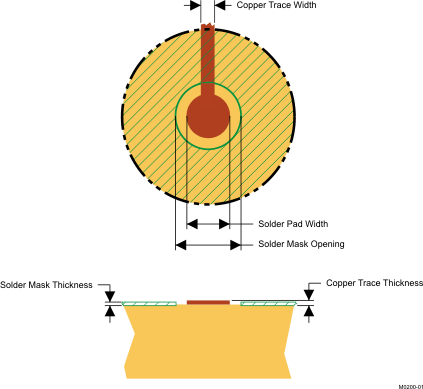
 Figure 23. Recommended Land Pattern Image and Dimensions
| SOLDER PAD DEFINITIONS(1)(2)(3)(4) | COPPER PAD | SOLDER MASK (5)
OPENING |
COPPER THICKNESS | STENCIL (6)
OPENING |
STENCIL THICKNESS |
|---|---|---|---|---|---|
| Non-solder-mask defined (NSMD) | 0.30mm | 0.360mm | 1oz max (0.032mm) | 0.34mm diameter | 0.1mm thick |
(1) Circuit traces from non-solder-mask defined PWB lands should be 75μm to 100μm wide in the exposed area inside the solder mask opening. Wider trace widths reduce device stand off and affect reliability.
(2) Best reliability results are achieved when the PWB laminate glass transition temperature is above the operating the range of the intended application.
(3) Recommend solder paste is Type 3 or Type 4.
(4) For a PWB using a Ni/Au surface finish, the gold thickness should be less than 0.5mm to avoid a reduction in thermal fatigue performance.
(5) Solder mask thickness should be less than 20 μm on top of the copper circuit pattern.
(6) For best solder stencil performance use laser cut stencils with electro polishing. Chemically etched stencils give inferior solder paste volume control.