ZHCSA09F July   2012  – December 2022 ISO1540 , ISO1541

PRODUCTION DATA  

  1. 特性
  2. 应用
  3. 说明
  4. Revision History
  5. Pin Configuration and Functions
  6. Specifications
    1. 6.1  Absolute Maximum Ratings
    2. 6.2  ESD Ratings
    3. 6.3  Recommended Operating Conditions
    4. 6.4  Thermal Information
    5. 6.5  Power Ratings
    6. 6.6  Insulation Specifications
    7. 6.7  Safety-Related Certifications
    8. 6.8  Safety Limiting Values
    9. 6.9  Electrical Characteristics
    10. 6.10 Supply Current Characteristics
    11. 6.11 Timing Requirements
    12. 6.12 Switching Characteristics
    13. 6.13 Insulation Characteristics Curves
    14. 6.14 Typical Characteristics
      1.      Parameter Measurement Information
  7. Detailed Description
    1. 7.1 Overview
    2. 7.2 Functional Block Diagrams
    3. 7.3 Feature Description
    4. 7.4 Isolator Functional Principle
      1. 7.4.1 Receive Direction (Left Diagram of )
      2. 7.4.2 Transmit Direction (Right Diagram of )
    5. 7.5 Device Functional Modes
  8. Application and Implementation
    1. 8.1 Application Information
      1. 8.1.1 I2C Bus Overview
    2. 8.2 Typical Application
      1. 8.2.1 Design Requirements
      2. 8.2.2 Detailed Design Procedure
      3. 8.2.3 Application Curve
  9. Power Supply Recommendations
  10. 10Layout
    1. 10.1 Layout Guidelines
      1. 10.1.1 PCB Material
    2. 10.2 Layout Example
  11. 11Device and Documentation Support
    1. 11.1 Documentation Support
      1. 11.1.1 Related Documentation
    2. 11.2 Related Links
    3. 11.3 Receiving Notification of Documentation Updates
    4. 11.4 Community Resources
    5. 11.5 Trademarks
  12. 12Mechanical, Packaging, and Orderable Information

Typical Characteristics

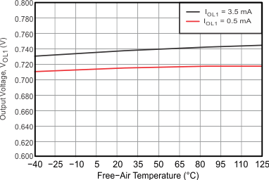
GUID-7B741928-E0A1-405E-821D-BECC2291412E-low.gif
Figure 6-2 Side 1: Output Low Voltage vs Free-Air Temperature
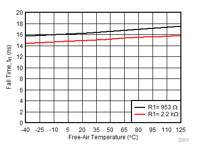
GUID-928CC5C0-4D27-45FD-8F2B-4934D1009734-low.gif
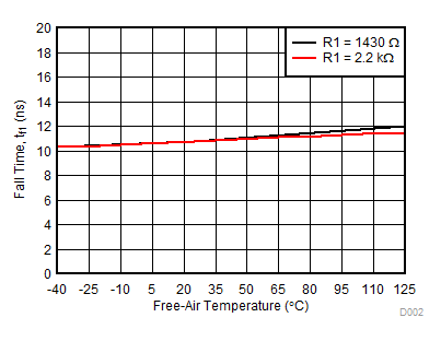
VCC1 = 3.3 VC1 = 40 pF
Fall time measured from 70% to 30% VCC1
Figure 6-4 Side 1: Output Fall Time vs Free-Air Temperature
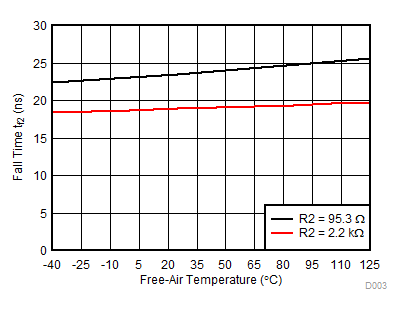
GUID-163D73C2-C88A-4D5E-846C-BCE78CE7E099-low.gif
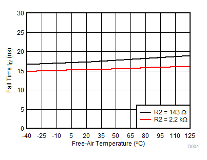
VCC2 = 3.3 VC2 = 400 pF
Fall time measured from 70% to 30% VCC2
Figure 6-6 Side 2: Output Fall Time vs Free-Air Temperature
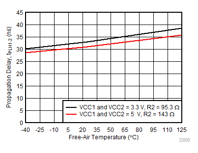
GUID-0AFF8EF3-488F-4001-B2F5-8DA6ADA02AD7-low.gif
C2 = 10 pF
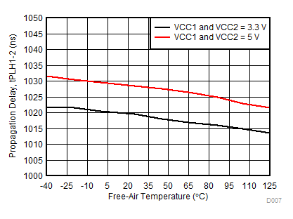
Figure 6-8 tPLH1-2 Propagation Delay vs Free-Air Temperature
GUID-45720B39-E69A-451A-9C59-FEC159E36435-low.gif
R2 = 2.2 kΩC2 = 400 pF
Figure 6-10 tPLH1-2 Propagation Delay vs Free-Air Temperature
GUID-643DABE2-6986-4D89-A33B-1E1B1DC4D2C4-low.gif
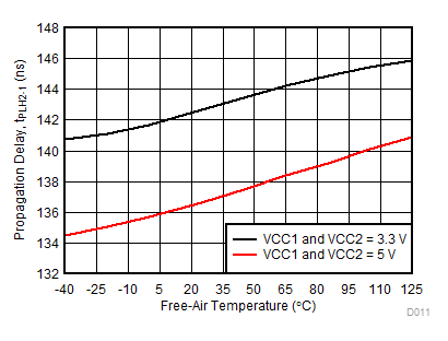
C1 = 10 pF
Figure 6-12 tPLH2-1 Propagation Delay vs Free-Air Temperature
GUID-F94C7176-3B48-460D-BD03-5304FE4C184B-low.gif
R1 = 2.2 kΩC1 = 40 pF
Figure 6-14 tPLH2-1 Propagation Delay vs Free-Air Temperature
GUID-3775E9ED-B114-4D57-801C-55B7C47CCDC1-low.gif
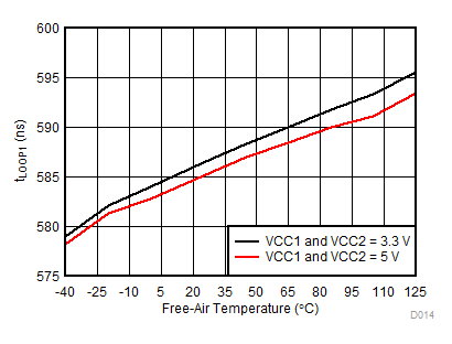
C1 = 40 pFC2 = 400 pF
Figure 6-16 tLOOP1 vs Free-Air Temperature
GUID-D543A6A3-3736-46D7-A143-9771F8F423FE-low.gif
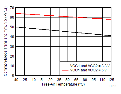
Figure 6-18 CMTI vs Free-Air Temperature
GUID-BE487CC0-6993-4B32-8546-A8ABACAB7B98-low.gif
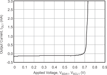
TA = 25°C
Figure 6-3 Side 1: Output Low Current vs SDA1 or SCL1 Applied Voltage
GUID-9E6FC794-0CDD-47B7-B915-4B34D6093738-low.gif
VCC1 = 5 VC1 = 40 pF
Fall time measured from 70% to 30% VCC1
Figure 6-5 Side 1: Output Fall Time vs Free-air Temperature
GUID-969AC993-D9A3-4979-B193-F4956458878A-low.gif
VCC2 = 5 VC2 = 400 pF
Fall time measured from 70% to 30% VCC2
Figure 6-7 Side 2: Output Fall Time vs Free-Air Temperature
GUID-5F1FF335-3C36-48F0-BFA8-5427120CD4F4-low.gif
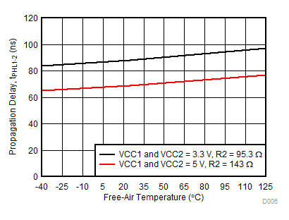
C2 = 10 pF
Figure 6-9 tPHL1-2 Propagation Delay vs Free-Air Temperature
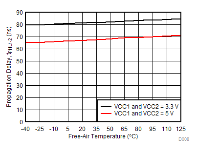
GUID-40E42040-A6A3-4377-8628-16F1CD1ACD92-low.gif
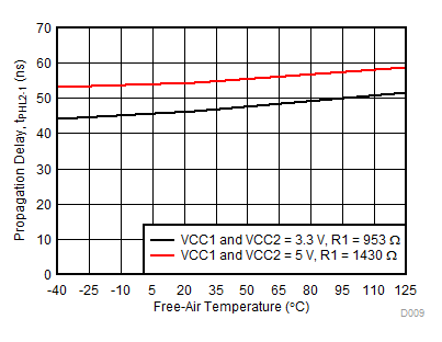
R2 = 2.2 kΩC2 = 400 pF
Figure 6-11 tPHL1-2 Propagation Delay vs Free-Air Temperature
GUID-6C183894-9536-4387-A23E-F2765D24D5E3-low.gif
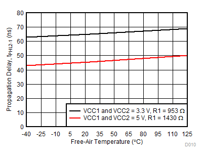
C1 = 10 pF
Figure 6-13 tPHL2-1 Propagation Delay vs Free-Air Temperature
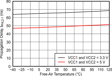
GUID-A3D0C3E9-3F93-4BE1-8981-7C4AE76B1655-low.gif
R1 = 2.2 kΩC1 = 40 pF
Figure 6-15 tPHL2-1 Propagation Delay vs Free-Air Temperature
GUID-C892B904-8C2E-463C-8F25-FD31A1212C78-low.gif
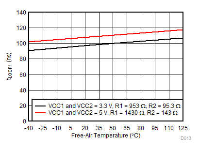
C1 = 40 pFC2 = 400 pF
R1 = 2.2 kΩR2 = 2.2 kΩ
Figure 6-17 tLOOP1 vs Free-Air Temperature