ZHCSAC2C August   2012  – October 2018 PCM5121 , PCM5122

PRODUCTION DATA.  

  1. 特性
  2. 应用
  3. 说明
    1.     Device Images
      1.      简化系统图
  4. 修订历史记录
  5. Device Comparison
  6. Pin Configuration and Functions
    1. 6.0.1 RHB Package I2C Mode (MODE1 tied to DGND and MODE2 tied to DVDD) Top View
    2. 6.0.2 RHB Package SPI Mode (MODE1 tied to DVDD) Top View
    3. 6.0.3 RHB Package Hardwired Mode (MODE1 tied to DGND, MODE2 tied to DGND) Top View
    4.     Pin Functions
  7. Specifications
    1. 7.1 Absolute Maximum Ratings
    2. 7.2 ESD Ratings
    3. 7.3 Recommended Operating Conditions
    4. 7.4 Thermal Information
    5. 7.5 Electrical Characteristics
    6. 7.6 Timing Requirements: SCK Input
    7. 7.7 Timing Requirements: XSMT
    8. 7.8 Switching Characteristics
    9. 7.9 Typical Characteristics
  8. Detailed Description
    1. 8.1 Overview
    2. 8.2 Functional Block Diagram
    3. 8.3 Feature Description
      1. 8.3.1 Terminology
      2. 8.3.2 Audio Data Interface
        1. 8.3.2.1 Audio Serial Interface
        2. 8.3.2.2 PCM Audio Data Formats
        3. 8.3.2.3 Zero Data Detect
      3. 8.3.3 XSMT Pin (Soft Mute / Soft Un-Mute)
      4. 8.3.4 Audio Processing
        1. 8.3.4.1 PCM512x Audio Processing
          1. 8.3.4.1.1 Overview
          2. 8.3.4.1.2 Software
        2. 8.3.4.2 Interpolation Filter
        3. 8.3.4.3 Fixed Audio Processing Flow (Program 5)
          1. 8.3.4.3.1 Filter Programming Changes
          2. 8.3.4.3.2 Processing Blocks – Detailed Descriptions
          3. 8.3.4.3.3 Biquad Section
          4. 8.3.4.3.4 Dynamic Range Compression
          5. 8.3.4.3.5 Stereo Mixer
          6. 8.3.4.3.6 Stereo Multiplexer
          7. 8.3.4.3.7 Mono Mixer
          8. 8.3.4.3.8 Master Volume Control
          9. 8.3.4.3.9 Miscellaneous Coefficients
      5. 8.3.5 DAC Outputs
        1. 8.3.5.1 Analog Outputs
        2. 8.3.5.2 Recommended Output Filter for the PCM512x
        3. 8.3.5.3 Choosing Between VREF and VCOM Modes
          1. 8.3.5.3.1 Voltage Reference and Output Levels
          2. 8.3.5.3.2 Mode Switching Sequence, from VREF Mode to VCOM Mode
        4. 8.3.5.4 Digital Volume Control
          1. 8.3.5.4.1 Emergency Ramp-Down
        5. 8.3.5.5 Analog Gain Control
      6. 8.3.6 Reset and System Clock Functions
        1. 8.3.6.1 Clocking Overview
        2. 8.3.6.2 Clock Slave Mode With Master and System Clock (SCK) Input (4 Wire I2S)
        3. 8.3.6.3 Clock Slave Mode With BCK PLL to Generate Internal Clocks (3-Wire PCM)
        4. 8.3.6.4 Clock Generation Using the PLL
        5. 8.3.6.5 PLL Calculation
          1. 8.3.6.5.1 Examples:
            1. 8.3.6.5.1.1 Recommended PLL Settings
        6. 8.3.6.6 Clock Master Mode from Audio Rate Master Clock
        7. 8.3.6.7 Clock Master from a Non-Audio Rate Master Clock
    4. 8.4 Device Functional Modes
      1. 8.4.1 Choosing a Control Mode
        1. 8.4.1.1 Software Control
          1. 8.4.1.1.1 SPI Interface
            1. 8.4.1.1.1.1 Register Read and Write Operation
          2. 8.4.1.1.2 I2C Interface
            1. 8.4.1.1.2.1 Slave Address
            2. 8.4.1.1.2.2 Register Address Auto-Increment Mode
            3. 8.4.1.1.2.3 Packet Protocol
            4. 8.4.1.1.2.4 Write Register
            5. 8.4.1.1.2.5 Read Register
            6. 8.4.1.1.2.6 Timing Characteristics
      2. 8.4.2 VREF and VCOM Modes
    5. 8.5 Programming
  9. Application and Implementation
    1. 9.1 Application Information
    2. 9.2 Typical Application
      1. 9.2.1 Design Requirements
      2. 9.2.2 Detailed Design Procedure
      3. 9.2.3 Application Curve
  10. 10Power Supply Recommendations
    1. 10.1 Power Supply Distribution and Requirements
    2. 10.2 Recommended Powerdown Sequence
      1. 10.2.1 XSMT = 0
      2. 10.2.2 Clock Error Detect
      3. 10.2.3 Planned Shutdown
      4. 10.2.4 Unplanned Shutdown
    3. 10.3 External Power Sense Undervoltage Protection Mode
    4. 10.4 Power-On Reset Function
      1. 10.4.1 Power-On Reset, DVDD 3.3-V Supply
      2. 10.4.2 Power-On Reset, DVDD 1.8-V Supply
    5. 10.5 PCM512x Power Modes
      1. 10.5.1 Setting Digital Power Supplies and I/O Voltage Rails
      2. 10.5.2 Power Save Modes
      3. 10.5.3 Power Save Parameter Programming
  11. 11Layout
    1. 11.1 Layout Guidelines
    2. 11.2 Layout Example
  12. 12Register Maps
    1. 12.1 PCM512x Register Map
      1. 12.1.1 Detailed Register Descriptions
        1. 12.1.1.1 Register Map Summary
        2. 12.1.1.2 Page 0 Registers
        3. 12.1.1.3 Page 1 Registers
        4. 12.1.1.4 Page 44 Registers
        5. 12.1.1.5 Page 253 Registers
      2. 12.1.2 PLL Tables for Software Controlled Devices
      3. 12.1.3 Coefficient Data Formats
      4. 12.1.4 Power Down and Reset Behavior
  13. 13器件和文档支持
    1. 13.1 开发支持
    2. 13.2 文档支持
    3. 13.3 相关链接
    4. 13.4 接收文档更新通知
    5. 13.5 社区资源
    6. 13.6 商标
    7. 13.7 静电放电警告
    8. 13.8 术语表
  14. 14机械、封装和可订购信息

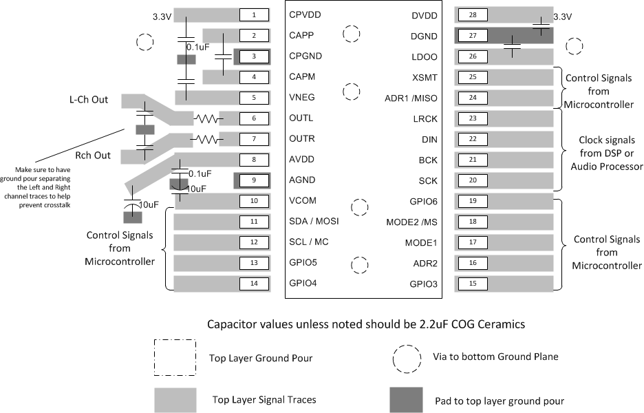
Layout Example

PCM5121 PCM5122 DatasheetLayoutExample_slas759.gif
It is recommended to place a top layer ground pour for shielding around the DAC and connect to lower main PCB ground plane by multiple vias
Figure 85. PCM514x Layout Example