ZHCSAC4B October   2012  – November 2017 SN65HVD82

PRODUCTION DATA.  

  1. 特性
  2. 应用
  3. 说明
  4. 修订历史记录
  5. Pin Configuration and Functions
  6. Specifications
    1. 6.1 Absolute Maximum Ratings
    2. 6.2 ESD Ratings
    3. 6.3 Recommended Operating Conditions
    4. 6.4 Thermal Information
    5. 6.5 Electrical Characteristics
    6. 6.6 Switching Characteristics
    7. 6.7 Typical Characteristics
  7. Parameter Measurement Information
  8. Detailed Description
    1. 8.1 Overview
    2. 8.2 Functional Block Diagram
    3. 8.3 Feature Description
      1. 8.3.1 Receiver Failsafe
      2. 8.3.2 Low-Power Standby Mode
    4. 8.4 Device Functional Modes
  9. Application and Implementation
    1. 9.1 Application Information
      1. 9.1.1 Device Configuration
      2. 9.1.2 Bus - Design
      3. 9.1.3 Cable-Length Versus Data Rate
      4. 9.1.4 Stub - Length
      5. 9.1.5 3-V to 5-V Interface
      6. 9.1.6 Noise Immunity
      7. 9.1.7 Transient Protection
    2. 9.2 Typical Application
      1. 9.2.1 Design Requirements
      2. 9.2.2 Detailed Design Procedure
        1. 9.2.2.1 Custom Design With WEBENCH® Tools
        2. 9.2.2.2 Isolated Bus Node Design
      3. 9.2.3 Application Curve
  10. 10Power Supply Recommendations
  11. 11Layout
    1. 11.1 Layout Guidelines
      1. 11.1.1 Design and Layout Considerations For Transient Protection
    2. 11.2 Layout Example
  12. 12器件和文档支持
    1. 12.1 器件支持
      1. 12.1.1 Third-Party Products Disclaimer
      2. 12.1.2 使用 WEBENCH® 工具定制设计方案
    2. 12.2 社区资源
    3. 12.3 商标
    4. 12.4 静电放电警告
    5. 12.5 Glossary
  13. 13机械、封装和可订购信息

Pin Configuration and Functions

D Package
16-Pin SOIC
(Top View)
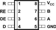
SN65HVD82 po_llsed6.gif

Pin Functions

PIN TYPE DESCRIPTION
NAME NO.
A 6 Bus input/output Driver output or receiver input (complementary to B)
B 7 Bus input/output Driver output or receiver input (complementary to A)
D 4 Digital input Driver data input
DE 3 Digital input Driver enable, active high
GND 5 Reference potential Local device ground
R 1 Digital output Receive data output
RE 2 Digital input Receiver enable, active low
VCC 8 Supply 4.5-V to 5.5-V supply