| INPUT CURRENTS |
| IIN |
Supply current from IN |
VDPM < VIN < VOVP AND VIN > VBAT+VSLP PWM switching, CE Enable |
|
13 |
|
mA |
| VDPM < VIN < VOVP AND VIN > VBAT+VSLP PWM switching, CE Disable |
|
|
5 |
| VIN= 5.5V, 0°C< TJ < 85°C, High-Z Mode |
|
170 |
225 |
μA |
| IBAT |
Battery discharge current in high impedance mode, (BAT, SW, SYS) |
0°C< TJ < 85°C, VBAT = 4.2 V,
VIN = 0V or 5V, High-Z Mode |
|
16 |
22 |
μA |
| Battery discharge current in SYSOFF mode |
0°C< TJ < 85°C, VBAT = 4.2 V,
VIN < UVLO, SYSOFF Mode |
|
|
1 |
| POWER-PATH MANAGEMENT |
| VSYSREG |
System Regulation Voltage |
MINSYS stage (no DPM or DPPM) |
–1% |
3.52 |
1% |
V |
| MINSYS stage (DPM or DPPM active) |
–1.50% |
VMINSYS
–200mV |
1.50% |
| BATREG stage |
|
VBAT
+ ICHG Ron |
|
| SYSREG stage |
VBATREG
+2.1% |
VBATREG
+3.1% |
VBATREG
+4.1% |
| VSPLM |
Enter supplement mode voltage threshold |
VBAT = 3.6V |
|
VBAT –
40mV |
|
V |
| ISPLM |
Exit supplement mode current threshold |
VBAT = 3.6V |
|
20 |
|
mA |
| tDGL(SC1) |
Deglitch Time, OUT Short Circuit during Discharge or Supplement Mode |
Measured from (VBAT – VSYS) = 300 mV |
|
740 |
|
μs |
| tREC(SC1) |
Recovery Time, OUT Short Circuit during Discharge or Supplement Mode |
|
|
64 |
|
ms |
| BATTERY CHARGER |
| RON(BAT-SYS) |
Internal battery charger MOSFET on-resistance |
Measured from BAT to SYS, VBAT = 4.2V (WCSP) |
|
20 |
30 |
mΩ |
| Measured from BAT to SYS, VBAT = 4.2V (QFN) |
|
30 |
40 |
| VBATREG |
I2C host mode |
Operating in voltage regulation, Programmable Range |
3.5 |
|
4.44 |
V |
| SA mode or I2C default mode |
|
|
4.2 |
|
|
| Voltage Regulation Accuracy |
TJ = 25°C |
–0.5% |
|
0.5% |
|
| TJ = 0°C to 125°C |
–0.75% |
|
0.75% |
|
|
| ICHG |
Fast Charge Current Range |
VLOWV ≤ VBAT < VBAT(REG) |
500 |
|
2000 |
mA |
|
Fast Charge Current Accuracy |
I2C mode |
–7% |
|
7% |
|
| ICHG-LOW |
Low Charge Current Setting |
Set via I2C |
297 |
330 |
363 |
mA |
| KISET |
Programmable Fast Charge Current Factor |
 |
232.5 |
250 |
267.5 |
AΩ |
| VISET |
Maximum ISET pin voltage (in regulation) |
|
|
0.42 |
|
V |
| RISET-SHORT |
Short circuit resistance threshold |
|
45 |
55 |
75 |
Ω |
| VLOWV |
Pre-charge to fast charge threshold |
Rising |
2.9 |
3 |
3.1 |
V |
| Hysteresis for VLOWV |
Battery voltage falling |
|
100 |
|
mV |
| IPRECHG |
Pr-charge current (VBATUVLO < VBAT < VLOWV) |
Ipre-chg is a precentile of the external fast charge settings. |
8 |
10 |
12 |
% |
| tDGL(LOWV) |
Deglitch time for pre-charge to fast charge transition |
|
|
32 |
|
ms |
| VBAT_UVLO |
Battery Under voltage lockout threshold |
VBAT rising |
2.37 |
2.5 |
2.63 |
V |
|
Battery UVLO hysteresis |
|
|
200 |
|
mV |
| VBATSHRT |
Trickle charge to pre-charge threshold |
|
1.9 |
2 |
2.1 |
V |
|
Hysteresis for VBATSHRT |
Battery voltage falling |
|
100 |
|
mV |
| IBATSHRT |
Trickle charge mode charge current (VBAT < VBATSHRT) |
|
25 |
35 |
50 |
mA |
| tDGL(BATSHRT) |
Deglitch time for trickle charge to pre-charge transition |
|
|
256 |
|
us |
| ITERM |
Termination Current Threshold |
Termination current on SA only |
|
10 |
|
%ICHG |
| Termination Current Threshold Tolerance |
|
–10% |
|
10% |
|
| tDGL(TERM) |
Deglitch time for charge termination |
Both rising and falling, 2-mV over-drive, tRISE, tFALL = 100 ns |
|
64 |
|
ms |
| VRCH |
Recharge threshold voltage |
Below VBATREG |
70 |
115 |
160 |
mV |
| tDGL(RCH) |
Deglitch time |
VBAT falling below VRCH, tFALL = 100 ns |
|
32 |
|
ms |
| BATTERY DETECTION |
| VBATREG_HI |
Battery Detection High Regulation Voltage |
Same as VBATREG |
|
VBATREG |
|
V |
| VBATREG_LO |
Battery Detection Low Regulation Voltage |
360 mV offset from VBATREG |
|
VBATREG
–480mV |
|
V |
| VBATDET Hi |
Battery detection comparator |
VBATREG = VBATREG_HI |
|
VBATREG
–120mV |
|
V |
| VBATDET LO |
Battery detection comparator |
VBATREG = VBATREG_LO |
|
VBATREG
+120mV |
|
V |
| IDETECT |
Battery Detection Current Sink |
Always on during battery detection |
|
7.5 |
|
mA |
| tDETECT |
Battery detection time |
For both VBATREG_HI and VBATREG_LO |
|
32 |
|
ms |
| Tsafe |
Safety Timer Accuracy |
|
–10% |
|
+10% |
|
| INPUT PROTECTION |
| IIN |
Input current limiting |
IIN_LIMIT = 100 mA |
90 |
95 |
100 |
mA |
| IIN_LIMIT = 150 mA |
135 |
142.5 |
150 |
|
| IIN_LIMIT = 500 mA |
450 |
475 |
500 |
|
| IIN_LIMIT = 900 mA |
810 |
860 |
910 |
|
| IIN_LIMIT = 1500 mA |
1400 |
1475 |
1550 |
|
| IIN_LIMIT = 2000 mA |
1850 |
1950 |
2050 |
|
| IIN_LIMIT = External |
 |
|
| ILIM |
Maximum input current limit programmable range for IN input |
|
500 |
|
2000 |
mA |
| KILIM |
Maximum input current factor for IN input |
ILIM = 500 mA to 2.0 A |
240 |
270 |
300 |
AΩ |
| VILIM |
Maximum ILIM pin voltage (in regulation) |
|
|
0.42 |
|
V |
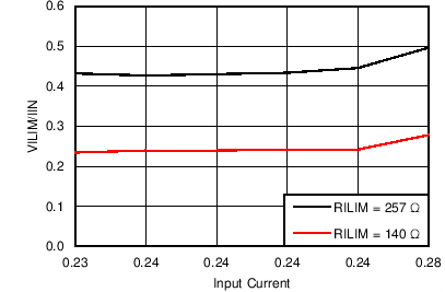
| IIN /IILIM |
Ratio between input current and the ILIM pin current in external control or stand alone mode |
External ILIM control or stand alone |
|
540 |
|
A/A |
| RILIM-SHORT |
Short circuit resistance threshold |
|
|
55 |
75 |
Ω |
| VIN_DPM |
VIN_DPM threshold range |
SA mode |
4.2 |
|
10 |
V |
| I2C mode |
4.2 |
|
4.76 |
| VIN_DPM threshold for USB Input in SA mode |
USB100, USB150, USB500, USB900, current limit selected. Also I2C register default. |
4.27 |
4.36 |
4.45 |
| VIN_DPM threshold with adaptor current limit and VDPM shorted to GND |
Must set to external resistor settings via the EN1/EN2 pins or the I2C register interface. |
VIN_DPM
.
–2% |
VIN_DPM |
VIN_DPM
.
+2% |
| VIN_DPM threshold Accuracy |
Both I2C and SA mode |
–2% |
|
2% |
|
| VREF_DPM |
DPM regulation voltage |
External resistor setting only |
1.15 |
1.2 |
1.25 |
V |
| VDPM_SHRT |
VIN_DPM short threshold |
If VDPM is shorted to ground, VIN_DPM threshold will use internal default value |
|
0.3 |
|
V |
| VUVLO |
IC active threshold voltage |
VIN rising |
3.15 |
3.35 |
3.5 |
V |
| IC active hysteresis |
VIN falling from above VUVLO |
|
175 |
|
mV |
| VSLP |
Sleep-mode entry threshold, VIN-VBAT |
2.0 V ≤ VBAT ≤ VBATREG, VIN falling |
0 |
50 |
100 |
mV |
| Sleep-mode exit hysteresis, VIN-VBAT |
2.0 V ≤ VBAT ≤ VBATREG |
40 |
100 |
160 |
mV |
| tDGL(SLP) |
Deglitch time for IN rising above VIN+VSLP_EXIT |
Rising voltage, 2-mV over drive, tRISE = 100 ns |
|
32 |
|
ms |
| VOVP |
Input supply OVP threshold voltage |
IN rising |
Input OVP
–200mV |
Input OVP |
Input OVP
+200mV |
V |
| VOVP hysteresis |
IN falling from VOVP |
|
100 |
|
mV |
| tDGL(OVP) |
Deglitch time for IN Rising above VOVP |
IN rising voltage, tRISE = 100 ns |
|
32 |
|
ms |
| VBOVP |
Battery OVP threshold voltage |
VBAT threshold over VBATREG to turn off charger during charge |
102.5 |
105 |
107.5 |
% VBATREG |
| VBOVP hysteresis |
Lower limit for VBAT falling from above VBOVP |
|
1 |
|
% VBATREG |
| tDGL(BOVP) |
BOVP Deglitch |
Battery entering/exiting BOVP |
|
1 |
|
ms |
| PWM CONVERTER |
| RON(BLK) |
Internal blocking MOSFET on-resistance |
Measured from IN to PMID (WCSP & QFN) |
|
60 |
100 |
mΩ |
| RON(HS) |
Internal high-side MOSFET on-resistance |
Measured from PMID to SW (WCSP & QFN) |
|
100 |
150 |
mΩ |
| RON(LS) |
Internal low-side MOSFET on-resistance |
Measured from SW to PGND (WCSP & QFN) |
|
110 |
165 |
mΩ |
| ICbC |
Cycle-by-cycle current limit |
VSYS shorted |
2.6 |
3.2 |
3.8 |
A |
| fOSC |
Oscillator frequency |
|
2.7 |
3 |
3.3 |
MHz |
| DMAX |
Maximum duty cycle |
|
|
95% |
|
|
| DMIN |
Minimum duty cycle |
|
0% |
|
|
|
| TSHTDWN |
Thermal trip |
|
|
150 |
|
°C |
| Thermal hysteresis |
|
|
10 |
|
|
| TREG |
Thermal regulation threshold |
Charge current begins to cut off |
|
125 |
|
|
| LDO (LINEAR DROPOUT) |
| VLDO |
LDO Output Voltage |
bq24251 and bq24253 |
VIN = 5.5 V, ILDO = 0 to 50 mA |
4.65 |
4.95 |
5.25 |
V |
| ILDO |
Maximum LDO Output Current |
|
50 |
|
|
mA |
| VDO |
LDO Dropout Voltage (VIN – VLDO) |
VIN = 5.0 V, ILDO = 50 mA |
|
200 |
300 |
mV |
| BATTERY-PACK NTC MONITOR (1) |
| VHOT |
High temperature threshold |
VTS falling |
29.6 |
30 |
30.4 |
% VLDO |
| VHYS(HOT) |
Hysteresis on high threshold |
VTS rising |
|
1 |
|
| VWARM |
Warm temperature threshold |
VTS falling |
37.9 |
38.3 |
38.7 |
| VHYS(WARM) |
Hysteresis on warm temperature threshold |
VTS rising |
|
1 |
|
| VCOOL |
Cool temperature threshold |
VTS rising |
56.1 |
56.5 |
56.9 |
| VHSY(COOL) |
Hysteresis on cool temperature threshold |
VTS falling |
|
1 |
|
| VCOLD |
Low temperature threshold |
VTS rising |
59.6 |
60 |
60.4 |
| VHYS(COLD) |
Hysteresis on low threshold |
VTS falling |
|
1 |
|
| VFRZ |
Freeze temperature threshold |
VTS rising |
62 |
62.5 |
63 |
| VHYS(FRZ) |
Hysteresis on freeze threshold |
VTS falling |
|
1 |
|
| VTS_DIS |
TS disable threshold |
|
70 |
|
73 |
| tDGL(TS) |
Deglitch time on TS change |
|
|
32 |
|
ms |
| INPUTS (EN1, EN2, EN2, CE, CE1, CE2, BATREG, SCL, SDA, DBP) |
| VIH |
Input high threshold |
|
1 |
|
|
V |
| VIL |
Input low threshold |
|
|
|
0.4 |
V |
| STATUS OUTPUTS (CHG, PG, STAT, INT, BATRDY) |
| VOL |
Low-level output saturation voltage |
IO = 5 mA, sink current |
|
|
0.4 |
V |
| IIH |
High-level leakage current |
Hi-Z and 5V applies |
|
|
1 |
µA |
| TIMERS |
| tSAFETY |
45 min safety timer |
|
|
2700 |
|
s |
| 6 hr safety timer |
|
|
21600 |
|
| 9 hr safety timer |
|
|
32400 |
|
| tWATCH-DOG |
Watch dog timer |
|
|
50 |
|
s |
| D+/D– DETECTION |
| IDP_SRC |
D+ current source for DCD |
DCD |
7 |
|
13 |
µA |
| RDM_DWN |
D– pull-down resistance for DCD |
DCD |
14.25 |
|
24.8 |
kΩ |
| VDP_LOW |
D+ low comparator threshold for DCD |
DCD |
0.85 |
0.9 |
0.95 |
V |
| VDP_SRC |
D+ source voltage for Primary Detection |
Primary Detection |
0.5 |
0.6 |
0.7 |
V |
| IDP_SRC_PD |
D+ source voltage output current for Primary Detection |
Primary Detection |
200 |
|
|
µA |
| IDM_SINK |
D– sink current for Primary Detection |
Primary Detection |
50 |
100 |
150 |
µA |
| VDAT_REF |
Primary Detection threshold |
Primary Detection |
250 |
325 |
400 |
mV |
| VLGC |
Primary Detection threshold |
Primary Detection |
0.85 |
0.9 |
0.95 |
V |
| VDM_SRC |
D- source voltage for Secondary Detection |
Secondary Detection |
0.5 |
0.6 |
0.7 |
V |
| IDM_SRC_PD |
D- source voltage output current for Secondary Detection |
Secondary Detection |
200 |
|
|
µA |
| IDP_SINK |
D+ sink current for Secondary Detection |
Secondary Detection |
50 |
100 |
150 |
µA |
| VDAT_REF |
Secondary Detection threshold |
Secondary Detection |
250 |
325 |
400 |
mV |
| VATT_LO |
Apple/TomTom detection low threshold |
Apple/TomTom Detection |
1.8 |
1.85 |
1.975 |
V |
| VATT_HI |
Apple/TomTom detection high threshold |
Apple/TomTom Detection |
3.2 |
3.5 |
3.8 |
V |
| CI |
Input Capacitance |
D– , switch open |
|
4.5 |
|
pF |
| D+, switch open |
|
4.5 |
|
| ID_LKG |
Leakage Current into D+/D– |
D–, switch open |
–1 |
|
1 |
µA |
| D+, switch open |
–1 |
|
1 |
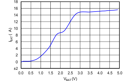
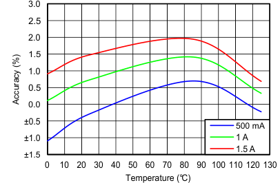
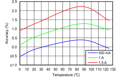 Figure 11. ICHG Accuracy with Internal Settings, VBAT = 3.3 V
